Market Insights: Rear-side passivation layers provide laser suppliers with first real opportunity in solar industry

Historically, the relationship between the solar photovoltaic (PV) industry and laser-based equipment suppliers has been in start-stop mode. On several occasions, the solar industry has been prioritized by the laser industry as a key end market, only for order intake to evaporate as manufacturing approaches were deemed uncompetitive or processing methods remained firmly rooted within research institutes.
In the past two years, however, the first real manufacturing-proven, laser-based process has emerged and is potentially on the verge of seeing widespread adoption. This new opportunity for laser-based tools has arisen because crystalline silicon (c-Si) manufacturers have focused on changing the composition of the rear side of solar cells through a process referred to as passivated emitter and rear contact (PERC) formation.
This article reviews the solar industry landscape at the start of 2016, identifies the key factors driving PV manufacturing technology, and considers the different issues impacting the near-term technology roadmap. The role of laser-based processes and tool suppliers is discussed in relation to these themes, including an explanation of why laser-based equipment has yet to truly impact solar cell manufacturing. Specifically, the PERC process is outlined in detail, in addition to potential laser-tool revenues on offer in the next 2–3 years.
The solar PV industry in 2016
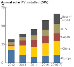
Year-on-year (Y/Y) growth for the solar PV industry has been taken for granted over the last decade, with the only question being whether annual deployment growth would be moderate (15–20% Y/Y) or strong (20–40%). Final figures accumulated for 2015 are expected to show that approximately 55-60 gigawatts (GW) of new capacity was installed, representing close to 25% growth compared to 2014. Similar growth rates are being forecast for 2016 (see Fig. 1).
Solar panels (or modules) today typically comprise 60 cells, with each cell measuring 156 × 156 mm and about 180 μm thick. Module power ratings for these 60-cell panels range between 250 and 300 W, with the best performing variants as high as 330–350 W. Residential installations of rooftop solar are typically using about 10–20 modules (2.5–5 kW), with larger commercial rooftops 100 kW to 1 MW. Ground-mounted (or utility-based) solar farms can range from 5 to 100 MW, with some of the largest in excess of 200 MW.
Solar cell production lines have increased in size from about 25 to 30 MW annual throughput in 2005 to approximately 60–100 MW in 2015, through a combination of single- and dual-lane tools. The leading cell producers are operating fabs with annual capacities at the 500 MW to 1 GW level, with the largest producers having total capacities in the 4–5 GW range. New equipment for a 100 MW production line is costing about $10–15 million today.
Driving the high double-digit growth is a complex mix of political, economic, and environmental factors across a wide range of countries, underpinned by the growing need for energy supply and the push towards decentralized non-carbon electricity generation. Having been stimulated by attractive government incentives (such as feed-in-tariffs in Europe, or the Investment Tax Credit system in the U.S.), the industry has undergone rapid price erosion, with modules declining to the current level of about 60c/W.
The fierce pricing environment over the past 3-5 years has seen various technologies being deemed uncompetitive, and has been a key factor in shifting manufacturing firmly to Asia and, in particular, China. Almost every cell manufacturer has gone through prolonged periods of negative operating metrics, leaving a small subset of producers (collectively known as the Silicon Module Super League) and technologies now set to drive the industry forward to the 100 GW-plus annual deployment phase (see Fig. 2).Laser industry flirtation with solar manufacturing
Most laser tool suppliers have at some stage allocated resources internally to determine the opportunity available from the solar industry. However, in reviewing market segmentations from laser suppliers when reporting quarterly or annual results, often no mention is afforded to contributions from solar.
The continued lure of solar to laser tool suppliers is not entirely unfounded. Most solar cells involve processing thin wafers of silicon, and production lines typically use thermal diffusion, deposition of thin layers, and fine patterning steps. In addition, the alternative technology to silicon-based solar cells is still thin-film manufacturing using glass substrates, employing deposition and fine-line patterning with selective material removal.
However, there are several reasons why lasers have not been considered essential tool types within the solar industry until now, despite many false starts over the past decade.
Most prominently, the one technology type that could not function without laser equipment, thin-film solar production, has been confined to a declining sub-5% market share today, with only two companies (First Solar, headquartered in Arizona, and Japanese-based Solar Frontier) left with meaningful capacity. Furthermore, both First Solar and Solar Frontier have changed strategies since being pure-play thin-film manufacturers by expanding operations downstream, where developing, operating, and selling power plants offers greater margins compared to upstream production. What is left from the thin-film solar sector, and specifically these two companies, to laser tool suppliers today would appear to be confined to tool upgrades.
Thin-film manufacturing using amorphous silicon-based layer deposition, previously considered to be the big opportunity for lasers, has been almost completely sidelined as a viable contender. What was largely an aspiration of flat panel display tool suppliers such as Applied Materials and ULVAC to drive solar manufacturers to adopt $100 million turn-key lines was ultimately shown to represent an offering with costs too high, efficiencies too low, and yield levels that were unacceptable.
With regards to the dominant c-Si cell technology (market share approximately 95%), laser-based tool suppliers saw initial traction back in 2006-2010 for edge isolation of front and back surfaces, through a scribing process around the front edges. However, this approach lost out ultimately to chemical wet etching at the rear side, with cell manufacturers preferring the simplicity of wet etch, a technology that is used almost exclusively for two other cell process stages (phosphosilicate glass removal and front surface texturing).
Lack of penetration with laser edge isolation saw laser tool suppliers engage then with more research-based and pilot-line processes, such as via drilling (for wrap-through cells) and phosphorous laser-doping (across various selective emitter configurations). Despite valiant efforts to aggressively transition some of these approaches from research to mass production, each was ultimately deemed too high-risk and with a level of complexity that was not needed. Furthermore, cost reduction was rapidly gripping an industry beset with declining stock prices, leaving no scope for manufacturing approaches that were unproven and would have a significant underutilization cost penalty on gross margins.
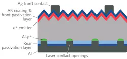
However, amongst the c-Si research activity was lurking a potential wildcard, in the form of rear-side laser openings that had been widely tipped as a prime candidate for future cell manufacturing, the tipping point for which was expected to be the widespread adoption of thin silicon wafers below 120 μm. This approach was coupled with the need to deposit passivation layers on the rear side of cells, necessitating a new means of forming rear contact openings, and is the basis for the current push for PERC-based solar cells (see Fig. 3).Status of PERC and opportunity for lasers
Interestingly, the main driver for PERC adoption was not the shift to thinner wafers, where the increase in rear side recombination losses would demand changing from the industry-standard screen-printed aluminum back surface field (Al-BSF) to one where passivation layers were required prior to contact forming. With the exception of just two manufacturers (SunPower and Panasonic), cell production has largely stuck to 180 μm wafers, with the requirement to reduce thickness negated by the decline in polysilicon prices from over $400/kg in 2008 to levels near $15/kg today.
Rather, PERC has become a focus for manufacturers today because of factors other than wafer thickness. During 2010-2014, wafer and cell manufacturers have been steadily improving cell efficiencies, increasing 60-cell multi c-Si module ratings from 235 to 260 W. This has been achieved by optimizing the multi c-Si ingot casting stage to create higher-quality wafer supply, and by cell makers improving performance through front-side enhancements, including using lower quantities of higher-quality silver paste while printing contact lines with higher aspect ratios. Module manufacturing has improved also, mainly through the change from two busbars to multi-busbar designs.
With options for any further wafer and front-surface cell enhancements more difficult to achieve, the obvious-and perhaps only-route on offer to cell makers at the end of 2014 was, in the absence of switching to a high-risk advanced design, to start making changes to the rear side of the cell. Consequently, during 2015 in particular, PERC has become prioritized as a mainstream contender for the next phase of cell efficiency gains.
PERC mainly involves adding two new process stages: depositing a passivation layer on the rear surface typically from plasma-enhanced chemical vapor deposition (PECVD), and opening contacts with lasers. While there are various options to the deposition stage (including atomic layer deposition), the contact opening is exclusively using lasers today. Currently, the supply of PERC laser tools has been confined to a relatively small group of suppliers, including European-based Innolas Solutions and 3D-Micromac. Other supply has come from domestic Chinese and Taiwan companies.
In terms of revenues on offer, upgrading a 1 GW fab to PERC is seeing revenues in the range of $10–20 million allocated to laser-based equipment, depending on tool supply from either Europe or Asia. Of the current 60 GW of c-Si-based capacity in the industry, about 20 GW can be considered as high potential for PERC upgrades in the next couple of years, suggesting laser tool revenues of approximately $300 million out to 2018.
Barriers remaining for widespread PERC adoption
One of the largest obstacles for PERC is that approximately 80% of p-type c-Si cells are using multi c-Si wafers, and the upgrade route on multi c-Si cells is harder compared to using mono c-Si cells. Nonetheless, two of the leading c-Si cell producers using multi c-Si wafers have already incorporated PERC upgrades into most of their multi-gigawatt cell capacities, suggesting that processing knowledge for volume manufacturing has been achieved, albeit outside China at this point.
Most of the leading c-Si module suppliers (the Silicon Module Super League of Canadian Solar, Hanwha Q CELLS, JA Solar, JinkoSolar, Trina Solar, and Yingli Green) are sold out for much of 2016, suggesting there is no immediate need to perform wholesale tool retrofits to their existing multi-gigawatt cell capacities. Furthermore, most of this capacity is multi c-Si cell-based, and still located in China.
Therefore, the time window for PERC to become mainstream may occur over longer time periods than hoped for—up to 5 years in some cases. If this occurs, then the real threat to PERC, and laser tool supply, may arise from alternative approaches to increasing cell efficiencies and any possible transition to higher performing n-type wafer supply.
About the Author
Finlay Colville
Dr. Finlay Colville has been Head of Research at PV-Tech and Solar Media Ltd since 2015. Before this, he spent 5 years as VP and head of solar at market research firm NPD Solarbuzz, and 10 years in various sales and marketing roles at Coherent, Inc. Dr. Colville holds a BSc in Physics from the University of Glasgow and a PhD in nonlinear photonics from the University of St. Andrews.


