Nanolithography: Laser bubble-pen lithography patterns colloidal nanoparticles

Colloidal particles such as quantum dots and metallic nanoparticles are emerging as important devices for applications in microelectronics, renewable energy, and sensing/drug delivery in the medical field. Unfortunately, standard lithography methods using photons, focused ion beams, or electron beams cannot pattern these particles on a solid substrate. Optical tweezers offer powerful capability for versatile manipulation of particles, but it is still challenging to immobilize the particles onto the substrate. Also, the high-power operation (up to 100 mW/μm2) limits its applications.
A unique method developed by researchers at the University of Texas at Austin uses a much-lower-power laser to create a microbubble at the interface between a plasmonic substrate and the liquid solution containing colloidal nanoparticles. This "bubble pen" uses convection, surface tension, and gas pressure to draw particles towards the bubble. Arbitrary patterns with different resolutions and architectures can be optically written on the substrate through this bubble-pen lithography (BPL) technique.
Plasmon-enhanced photothermal effects
Nanoparticles with sizes on the order of tens of nanometers with single-digit nanometer spacings on a glass slide are used as the plasmonic substrate. Low-power lasers with single-digit milliwatts per square micrometer levels and with wavelengths tuned to match the plasmon resonance wavelength of the nanoparticles are adequate for patterning.
To form the bubbles, a 2-μm-diameter laser beam is focused from the underside of a plasmonic substrate onto which a solution of colloidal particles is sandwiched between the substrate and a cover slip with a 120 μm spacer. Because of water vaporization from plasmon-enhanced photothermal effects, a bubble with a diameter down to 1 μm is formed on top of the plasmonic substrate.
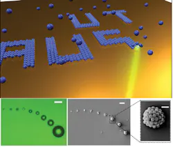
The colloidal particles are then dragged towards the microbubble, trapped on the bubble/solution interface, and immobilized on the substrate. When the laser power is off, the particles remain at the location they were patterned because of the enhanced substrate adhesion by the thermal effect. These particle patterns remain even after the substrate is rinsed and dried, making the method applicable to the fabrication of functional devices. Using the laser beam as a pen, a pattern of nanoparticles is formed by moving the bubble as the laser beam is scanned (see figure).
Particle trapping at the microbubbles is because of a combination of natural convection caused by the temperature gradient on the substrate and Marangoni convection induced by the surface-tension gradient along the microbubble surface. The in-plane drag force of the bubble attracts the particle, trapping it when it touches the microbubble surface—a phenomenon quantified and predicted by force equations. In fact, the temperature distribution of the bubble can also be predicted by computational fluid dynamics (CFD) simulations.
In further experiments, lasers with different power densities can be used to create different-sized bubbles that can actually incorporate nanoparticles such as polystyrene beads onto the bubble in a sort of three-dimensional (3D) shell configuration at laser power levels around 1 mW/μm2—100X less power than typical optical tweezers.
"The patterned particles have a variety of applications depending on the types of the particles. For example, metal nanoparticles can lead to metasurfaces and metamaterials that can manipulate light in a way that natural materials cannot afford, and patterned biological cells will find important applications in tissue engineering and high-throughput drug screening," says Yuebing Zheng, assistant professor at the University of Texas at Austin. "Our future work will further improve the throughput and automation of the technique for high-volume manufacturing of functional materials and devices with colloidal particles and biological cells. One of the approaches will be to develop multiple-beam processing."
REFERENCE
1. L. Lin et al., Nano Lett., 16, 1, 701–708 (2016); doi:10.1021/acs.nanolett.5b04524.
About the Author

Gail Overton
Senior Editor (2004-2020)
Gail has more than 30 years of engineering, marketing, product management, and editorial experience in the photonics and optical communications industry. Before joining the staff at Laser Focus World in 2004, she held many product management and product marketing roles in the fiber-optics industry, most notably at Hughes (El Segundo, CA), GTE Labs (Waltham, MA), Corning (Corning, NY), Photon Kinetics (Beaverton, OR), and Newport Corporation (Irvine, CA). During her marketing career, Gail published articles in WDM Solutions and Sensors magazine and traveled internationally to conduct product and sales training. Gail received her BS degree in physics, with an emphasis in optics, from San Diego State University in San Diego, CA in May 1986.