Silicon Photonics: Design approach to integrated photonics explores entire space of fabricable devices

ALEXANDER Y. PIGGOTT, JESSE LU, and JELENA VUČKOVIĆ
The design of digital circuits is currently dominated by hardware-description languages such as Verilog and VHSIC Hardware Description Language (VHDL). This automation of circuit design has enabled the development of modern computer processors with billions of transistors.
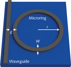
Integrated photonic devices, on the other hand, are still designed by hand. A designer first picks a basic design based on analytic theory with a handful (two to six) of free parameters. A canonical example would be the microring resonator (see Fig. 1), commonly used as a narrow spectral filter. The design is simple, with only a few adjustable parameters: the radius (r) of the ring, the width (w) of the waveguides, and the gap (g) between the ring and the waveguide. The designer then tunes these parameters by running many optical simulations. This brute-force approach is inefficient and limits the designer to a small library of known devices.
Arbitrary photonic devices
What if, however, we were able to search the full space of fabricable devices? If we could do this successfully, we would be guaranteed to improve device performance and shrink device sizes. Unfortunately, the space of fabricable devices is absolutely enormous. For example, suppose we want to design a silicon photonics device with a 1 × 1 μm design region. If we divide it into 0.1 × 0.1 μm pixels, easily achievable with modern nanofabrication, and allow each pixel to either contain silicon (1) or not (0), then we have 2100 ≈ 1030 possible devices.
We can draw two key insights about full-freedom design from this example. First, full-freedom design must be automated. A human designer would specify the device performance, but the actual design must be performed by a computer algorithm. Secondly, a simple brute-force search of all possible devices is intractable. Far more efficient design methods are necessary.
Ideally, we'd want an optimization algorithm whose computational cost is independent of the number of free parameters in the design. This would allow us to design devices that exploit the full space of fabricable devices. Thankfully, it turns out that such optimization methods exist. Related methods have long been used in other fields such as aerospace design and machine learning, but they were only recently introduced to optical design.
Design algorithms
Our research group uses two such methods to design arbitrary photonic devices. We first generate an initial guess for our structures using a so-called objective first design method.1 In this method, we initially allow our electromagnetic fields to be unphysical, but force them to satisfy any performance constraints we may have. We then iteratively reduce any violation of Maxwell's equations by modifying both the structure and electromagnetic fields. Since we prioritize our performance objectives over Maxwell's equations, we call this method "objective first."
Next, we fine-tune our structures using the adjoint optimization method, which has also been studied by a number of other groups in the context of optical devices.2-4 The key idea is that the gradient of a performance metric can be efficiently computed by simulating a single adjoint problem. This gradient can then be used in steepest-descent optimization. Adjoint optimization is essentially the opposite of the objective first method: here, we force Maxwell's equations to hold, and then try to minimize the violation of our performance constraints.
The vast majority of the computational cost for both methods comes from running a handful of electromagnetic simulations (as few as two) on each iteration. Critically, the number of simulations run on each iteration is completely independent of the number of free design parameters. This makes the objective first method and adjoint optimization far more efficient than heuristic methods such as genetic algorithms and particle swarm optimization, whose computational cost is proportional to the number of free parameters.
Both the objective first and adjoint optimization methods are iterative methods that converge on some local optimum. As such, neither method can find the globally optimal device for any given problem. However, by massively opening up the parameter space, we found that we can design devices with higher performance or a much smaller size than those designed using traditional methods.
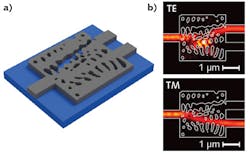
One such device we designed using our algorithm is a TE/TM polarization splitter (see Fig. 2).1 This device splits the two incident polarizations of light into separate output waveguides within a footprint of 2.8 × 2.8 μm. In simulations, it has an insertion loss of only 0.9 dB and a crosstalk of less than 19 dB.Experimental demonstration
As a proof of concept, we designed and experimentally tested a compact demultiplexer for telecommunications wavelengths (see Fig. 3).5 This silicon photonics device splits 1300 nm and 1550 nm light with a device footprint of only 2.8 × 2.8 μm. The demultiplexer has an insertion loss of 2 to 4 dB, crosstalk less than 11 dB, and a 3 dB bandwidth greater than 100 nm.We also found that our demultiplexer was robust to fabrication imperfections. Despite being fabricated with minimal process control, our fabricated devices had highly repeatable performance (see Fig. 2). We achieved this by designing the device to be broadband, which we found was a good heuristic for fabrication robustness.1
Advanced optimization methods, combined with recent improvements in computational power, have started to change how we design integrated photonics devices. Using these methods, researchers have recently designed devices that can radiatively cool themselves below ambient air temperature even when exposed to direct sunlight,6 or can make incandescent light bulbs nearly as efficient as LEDs.7 In the future, we can expect sophisticated optimization methods such as our objective first method to revolutionize the photonics industry, enabling a new generation of extremely compact and high-performance optics.
REFERENCES
1. J. Lu and J. Vučković, Opt. Express, 21, 11, 13351–13367 (2013); doi:10.1364/oe.21.013351.
2. C. M. Lalau-Keraly et al., Opt. Express, 21, 18, 21693–21701 (2013); doi:10.1364/oe.21.021693.
3. A. C. R. Niederberger et al., Opt. Express, 22, 11, 12971–12981 (2014); doi:10.1364/oe.22.012971.
4. J. S. Jensen and O. Sigmund, Laser Photon. Rev., 5, 308–321 (2011); doi:10.1002/lpor.201000014.
5. A. Y. Piggott et al., Nature Photon., 9, 6, 374–377 (2015); doi:10.1038/nphoton.2015.69.
6. A. P. Raman et al., Nature, 515, 540–544 (2014); doi:10.1038/nature13883.
7. O. Ilic et al., NatureNanotechnol., published online Jan. 11, 2016; http://dx.doi.org/10.1038/nnano.2015.309.
Alexander Y. Piggott, Jesse Lu, and Jelena Vučković are at the Ginzton Laboratory of Stanford University, Stanford, CA; e-mail: [email protected]; https://ginzton.stanford.edu.

