Integrated Photonics: Fin optical waveguide will aid co-integration of photonics with electronics
The ability of an integrated-photonics optical waveguide to confine light is ordinarily created by building the waveguide atop a continuous layer of low-refractive-index material, allowing the waveguide to channel light via total internal reflection. For example, in silicon photonics, a continuous layer of silicon dioxide (SiO2) is ordinarily placed underneath the network of silicon waveguides to allow them to function.
However, in silicon photonics, the fact that the low-index layer is continuous creates problems for the integration of photonics with electronics. In other types of integrated photonics, such as those based on III-V semiconductors, silicon carbide (SiC), or diamond, the required buried layer of low-index material weakens the structure and complicates fabrication.
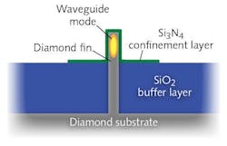
To solve this problem, Richard Grote and Lee Bassett, researchers at the Quantum Engineering Laboratory, Department of Electrical and Systems Engineering, University of Pennsylvania (Philadelphia, PA), have come up with a waveguide geometry that simultaneously allows confinement of light and a physical connection with the substrate of the same material (see figure).1
The fin is spanned by a low-index material in its lower portion and a higher-index material at its top, creating an effective index high enough to carry light at the top, but not in the lower portions. And the all-important physical connection to the substrate is maintained.
CMOS-compatible
For silicon photonics, the structure works with CMOS-compatible co-integration of the silicon photonic components with very large-scale integration (VLSI) electronics, such as those used in computer chips. For other types of integrated photonics, the arrangement provides strength and simplicity.
In one example, a diamond fin and substrate with a refractive index of about 2.4 and operating at a 637 nm wavelength are surrounded by a thick SiO2 buffer layer with an index of 1.45 and a thin (200 nm) silicon nitride (Si3N4) confinement layer with an index of 2.0 (see figure). Even though the refractive indices of both SiO2 and Si3N4 are below that of diamond, the fin still confines light. The reason is that the combination of indices in different regions creates differing effective indices, which are high enough for confinement in the Si3N4-affected region, but not in the SiO2 region.
If the waveguide fin itself is too narrow, it cannot carry the lowest-order mode; if it is too wide, light leaks out the bottom and down the fin into the substrate. If the confinement layer is too broad along the fin, a higher-order mode results. Proper confinement and propagation via the fundamental mode depends on a balance of geometry and effective indices. The resulting propagation loss because of substrate leakage is <0.15 dB/cm.
High-Q microring resonator
A circular fin waveguide can be used to create a microring resonator. For example, the bending loss for a diamond fin curved to a radius of 10 μm is <0.06 dB per 90° bend using a buffer layer thickness of 2.5 μm. This allows a 20-μm-diameter microring resonator to be made that has an unloaded quality factor Q >30,000.
In another example, a silicon waveguide fin with a SiO2/Si3N4 buffer/confinement structure is designed for single-mode propagation at the telecommunications wavelength of 1.55 μm. In this case, loss because of substrate leakage is calculated to be <1.0 dB/cm, and a 20-μm-diameter microring resonator of silicon would have a Q >10,000.
The researchers note that using the fin waveguide design in indium phosphide (InP)-based photonic integrated circuits would provide an alternative to the conventional indium gallium arsenide (InGaAs) guiding layer, resulting in higher confinement and a smaller mode area.
REFERENCE
1. R. R. Grote and L. C. Bassett, arXiv:1601.01239v1 [physics.optics] (Jan. 6, 2016).

John Wallace | Senior Technical Editor (1998-2022)
John Wallace was with Laser Focus World for nearly 25 years, retiring in late June 2022. He obtained a bachelor's degree in mechanical engineering and physics at Rutgers University and a master's in optical engineering at the University of Rochester. Before becoming an editor, John worked as an engineer at RCA, Exxon, Eastman Kodak, and GCA Corporation.
