Planar visible-region metalens is practical enough for real use in microscopy
The development of metalenses—lenses based on metamaterials, either 2D or 3D, rather than on bulk glass—has been pursued in the lab for years. The resulting devices have largely been interesting curiosities, having the advantages of extreme thinness and lightness, and sometimes the ability to image objects at somewhat beyond the diffraction limit because of their inclusion of evanescent electromagnetic waves in the imaging process. They also have the disadvantages of high loss, difficulty in fabrication, and, in many cases, poor imaging from even slight imperfections. The optics industry, which is based on practicality (not only must things work, but they must also be reasonably fabricable), will very carefully vet any new technology before putting it on the production line. Now, researchers at Harvard University (Cambridge, MA) and the University of Waterloo (Waterloo, ON, Canada) have developed a metalens that may get more than a first or second glance from the optics world.
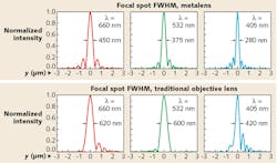
The metalens design, which is monochromatic and thus suited for laser light, is based on the conversion of right-handed, circularly polarized incident light to left-handed, circularly polarized light. Therefore, the nanostructure on the lens actually operates as a half-wave plate. The researchers fabricated an array of high-aspect-ratio titanium dioxide nanofins on a glass substrate, giving the nanofins a spatially varying rotation angle to produce the proper output phase profile. They created three metalenses with operating wavelengths of 660, 532, and 405 nm, respectively—all the lenses had a 240 μm diameter and a numerical aperture of 0.8 (focal length of 90 μm), resulting in three 170X objective lenses at the three respective wavelengths. When tested at their design wavelengths, all three metalenses produced diffraction-limited spots. Their full-width half-maximum (FWHM) focal spots were also compared to those produced by a state-of-the-art Nikon microscope objective; the metalens FWHMs were all smaller. Efficiencies of the metalenses at 405, 532, and 660 nm were high—86%, 73%, and 66%, respectively. Reference: M. Khorasaninejad et al., arXiv:1605.02248v1 [physics.optics] (May 7, 2016).

John Wallace | Senior Technical Editor (1998-2022)
John Wallace was with Laser Focus World for nearly 25 years, retiring in late June 2022. He obtained a bachelor's degree in mechanical engineering and physics at Rutgers University and a master's in optical engineering at the University of Rochester. Before becoming an editor, John worked as an engineer at RCA, Exxon, Eastman Kodak, and GCA Corporation.
