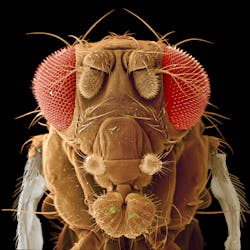
Novel Cameras: Ultrathin mobile cameras with facet optics are maturing

After years of ever-sharper displays and faster processors, cameras have become the main features of smartphones. Not only are there cameras on both sides, but also an increasing amount of two lenses on the flip side. However, such an advanced system comes at a price: there is a bump on the back cover. The engineers have reached the physical limits and more space for the lens modules is required. The physics here is simple—a higher resolution calls for larger chips and a wider aperture, which leads to bigger lenses and camera modules.
Engineers and physicists from the German Fraunhofer Society started to develop ultrathin camera systems in 2010, based on the "insect eye" principle (see frontis). The so-called facetVISION project is a collaboration between the Fraunhofer Institute for Applied Optics and Precision Engineering (IOF) in Jena and the Fraunhofer Institute for Integrated Circuits (IIS) in Erlangen. The developers have already been granted about 50 patents related to their ultrathin camera technology.
Insect eye cameras
Many animals, such as birds and mammals, share the same basic setup in their optical systems: a single lens that focuses incoming light onto a sensory area. With its spherical geometry, this seems to be an almost perfect optical system. First analog and then digital camera systems followed that idea, although with two tradeoffs—the sensor was flat, and the lens soon became a set of lenses to enable zooming and compensate for aberrations.
In the quest for better digital photography, the race toward ever-higher resolution has already reached the physical limits of the medium. The increasing resolution scales with decreasing pixel size on the imaging sensors. However, with a smaller pixel size, the noise increases. Now, with pixel sizes as small as 1.1 μm, the level of noise has become critical and disturbs the image quality to a greater degree than can be compensated for by the image processors. Added to this, pixels that are smaller than 1 μm would be smaller than the diffraction limit for visible light, which would also cause problems.
Despite all this, the high resolution of cameras and, increasingly, of mobile cameras is a crucial sales point, meaning that larger sensors are required. It is self-evident that a larger sensor area calls for a greater lens diameter. If we increase the diameter of spherical optics, we automatically increase their thickness at the same time, and the sophisticated systems in modern smartphones consist of five or six such elements. With a larger sensor needing a thicker lens module, there seems to be no way around the problem if we stick to conventional optics.
The inspiration for an alternative solution comes to our researchers from an entirely different group of animals: insects. By nature, these creatures are small and, accordingly, their optical systems are optimized for reduced volumes. The workhorse of biomedical research, the fruit fly Drosophila melanogaster, is 2-3 mm long and therefore has an eye that is much smaller than 1 mm. Basically, it consists of many small lenses, with a sensor behind each one. While it offers a large field of view, its angular resolution is rather low (see Fig. 1).Testing wafer-level technologies for manufacturing
Conventional lenses for mobile camera modules are usually produced via injection-molding processes. Such lenses, which have diameters of a few millimeters, are made from special polymers and aligned into miniature optical systems.
Alternatively, optics for bio-inspired ultrathin cameras can be made as arrays of sub-millimeter lenslets. These can be produced in large quantities using wafer-level UV-replication techniques. Costs are low and processes traditionally used in microelectronics manufacturing appear favorable for implementation.
To test these ideas, the Fraunhofer team developed a prototype of the camera module with HD resolution (720p or 1280 × 720 pixels; see Fig. 4). With a particular focus on manufacturability, external partners were contracted to produce 1250 of these modules using commercial CMOS image sensors in a pilot series. While the technical parameters satisfied the expectations, the costs were similar to those of conventional modules.Further research revealed challenges with the upscaling of the micro-optics. Sensors in the multi-megapixel (Mpixel) range are available with pixel sizes down to almost 1 μm. Manufacturing of appropriate lenslets turned out to be difficult, and at the least expensive. In the end, the technology appeared to be competitive up to resolutions of about 4 Mpixels, but not for larger sensor resolutions.
Paving the way toward 20 Mpixels
The flat camera module represented a window of opportunity in the market, but the resolution limitations—without significant cost advantages—led the team to rethink its approach. One question was crucial: was there a solution with the benefits of both worlds? The main advantage of the insect eye technique is its segmentation of the field of view, allowing for thinner optics. What would happen if we were to move closer to the one-lens idea and use just a few lenses imaged onto larger sensors, instead of thousands of lenslets?
To answer this question, the researchers tested a new system with four optical channels and, using their experience from the microlens systems, were able to extract an excellent image. A dual array with two of these four channels systems was still 50% lower than a conventional camera module. Since proven large scale lens manufacturing processes like injection molding can be used, lower costs compared to conventional optics are expected, while preserving the benefit of reduced camera height.
Given that the micro-lenses were no longer a technological limitation, this opened the way to larger sensor sizes and higher resolutions. A system with a 13 Mpixel sensor is currently under development, and larger resolutions of up to 20 Mpixels will follow by the end of the 2016. The use of conventional manufacturing processes will also facilitate the integration of proven features, such as autofocus and optical image stabilization.
At this point, current mobile devices use separate cameras for the user side and the flip side. The new module would allow for some interesting changes, such as one camera module for both sides.
The future of facet optics
Implementation of the bio-inspired idea of facet optics for mobile imaging has entailed a long learning curve. The current state of technical development is an optical system that shows a height <5 mm for sensor resolutions of up to 20 Mpixels, while retaining an aperture of f/2. Inherent features such as depth mapping or after-shot refocusing will cater to upcoming trends in mobile imaging.While the main focus of the development has been on mobile imaging, there are also other opportunities presenting themselves. For example, the growing trend of automated driving will increase the demand for thin cameras, as well as for spatial imaging systems. In this case, the implementation of wafer-level optics would be very suitable since it uses a different polymer for its lenses, which can tolerate automotive-grade temperatures.
ACKNOWLEDGEMENT
The facetVISION initiative is funded by the Fraunhofer-Zukunftsstiftung (Fraunhofer Research Foundation), an organization that invests in future-oriented strategic projects of the Fraunhofer Society.
Kevin Füchsel | Head of Department Strategy & Marketing, Fraunhofer IOF
Kevin Füchsel is head of department strategy & marketing at the Fraunhofer Institute for Applied Optics and Precision Engineering (Fraunhofer IOF; Jena, Germany).
Andreas Tünnermann
Andreas Tünnermann is director of the Fraunhofer Institute for Applied Optics and Precision Engineering (Fraunhofer IOF), as well as a professor in physics and director of the Institute of Applied Physics at Friedrich Schiller University (both in Jena, Germany).

Andreas Thoss | Contributing Editor, Germany
Andreas Thoss is the Managing Director of THOSS Media (Berlin) and has many years of experience in photonics-related research, publishing, marketing, and public relations. He worked with John Wiley & Sons until 2010, when he founded THOSS Media. In 2012, he founded the scientific journal Advanced Optical Technologies. His university research focused on ultrashort and ultra-intense laser pulses, and he holds several patents.


