Gas Sensing: PIC filters and SLEDs progress towards low-cost, mid-IR multi-gas sensor

Superluminescent light-emitting diode (SLED) source technology from the Optoelectronics Research Centre at the Tampere University of Technology (Tampere, Finland), silicon (Si) photonic integrated circuit (PIC) expertise from the VTT Technical Research Centre of Finland (Espoo, Finland), molded mid-infrared (mid-IR) lenses from ITME (Warsaw, Poland), and gas-sensing technologies from industrial partners GasSecure (Oslo, Norway), Vaisala (Vantaa, Finland), Airoptic (Poznan, Poland), and VIGO (Ozarow, Poland) are being used in the Horizon 2020 European consortium project MIREGAS in the development of a tunable, mid-IR, low-cost multi-gas sensor.1 The MIREGAS project received a grant of $3.7 million dollars from Horizon 2020 via the Photonics Public Private Partnership.
As detailed in the MIREGAS project objectives, the mid-IR gas sensor goals are a 2.7–3.5 μm wavelength range using an SLED with a 100 nm bandwidth, 10X better signal-to-noise ratio (SNR) compared to thermal emitters, a Si PIC filtering technique to achieve gas-detection specificity, and 10X better spectral resolution of 1 nm compared to using conventional micro-opto-electromechanical system (MOEMS) filters, all at a manufacturing cost of about $315 per unit.
To date, the MIREGAS project has achieved of its intermediate goals by successfully developing a prototype 2.7 μm SLED light source packaged in a TO can equipped with a mid-IR lens and intermediate prototypes of the light source based on the PIC filter.
PICs and SLEDs
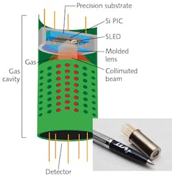
Gas sensing is accomplished, as in all other mid-IR sensors, by illuminating a gas sample with a collimated beam of light and analyzing the absorption lines present in the transmission spectrum.
To perform the spectral filtering function, several options have been demonstrated for MIREGAS: wavelength selection using two 1XN arrayed waveguide gratings (AWGs) and an array of switches; a demultiplexing (DEMUX) function using cascaded Mach-Zehnder interferometer (MZI) interleavers with 1 kHz modulation frequency, a DEMUX using angled multimode interference (MMI) structures, or a DEMUX using an echelle grating that reflects different input wavelengths in different waveguides placed at different angles.
The latter have been chosen as the best solution to match the requirements and specs coming from the end-users involved in the project consortium. Novel special reconfiguration approaches have been introduced, based both on tuning and switching, to identify gases through their unique fingerprints. A patent application is being submitted.
For the SLED source, ORC researchers first demonstrated a gallium antimonide (GaSb) SLED emitting at 2 μm using different waveguide designs that reaches several tens of milliwatts of output power compared to the submilliwatt levels typically seen for these sources. And more recently, the team demonstrated SLEDs emitting at 2.65 μm using two gallium indium arsenide antimonide (GaInAsSb) quantum wells embedded in lattice-matched aluminum GaAsSb (AlGaAsSb) waveguide and cladding layers on a GaSb substrate that reached an output power of nearly 0.5 mW with a 300 nm wide spectrum.
To form a collimated beam from the SLED, the MIREGAS project members are working to develop a new type of low-oxygen, heavy-metal-oxide glass that transmits mid-IR radiation and is formed in a molded-glass process called hot embossing. To date, molded-glass lenses that fit into a TO-can architecture have been experimentally produced.
Packaging and assembly of the tiny sensor involves submicron alignment of the SLED that is flip-chip bonded to the Si PIC, machine vision and active-alignment techniques for the molded-lens assembly together with epoxy bonding for 30 second assembly times and ±1 μm alignment precision, and the use of solder glasses and laser welding to bond the sensor components onto the TO header to create a hermetic package.
"The possibility to tailor the spectral output to match any wanted set of absorption lines with any desired bandwidth below 3500 nm is the major advantage of our light source when compared to the single narrow line of a tunable laser," says VTT research professor Pentti Karioja. "At first glance, this is advantageous for gas sensing, but further-on the light source will be used in all kinds of mid-IR sensors, for process analysis technology (PAT), environmental and food safety, and security applications, for example."
REFERENCE
1 See http://bit.ly/2iFD2jm.

Gail Overton | Senior Editor (2004-2020)
Gail has more than 30 years of engineering, marketing, product management, and editorial experience in the photonics and optical communications industry. Before joining the staff at Laser Focus World in 2004, she held many product management and product marketing roles in the fiber-optics industry, most notably at Hughes (El Segundo, CA), GTE Labs (Waltham, MA), Corning (Corning, NY), Photon Kinetics (Beaverton, OR), and Newport Corporation (Irvine, CA). During her marketing career, Gail published articles in WDM Solutions and Sensors magazine and traveled internationally to conduct product and sales training. Gail received her BS degree in physics, with an emphasis in optics, from San Diego State University in San Diego, CA in May 1986.