Full-color 3D meta-hologram is first step towards matrix-free 3D display
Holography has numerous applications in beam shaping, product authentication, and in the entertainment industry. Recognizing that the large pixel size, limited viewing angle, lack of full-color performance, and limited phase modulation ability of traditional holograms limits their potential, Xiangang Luo from the State Key Laboratory of Optical Technologies on Nano-fabrication and Micro-engineering (SKLOTNM) at the Chinese Academy of Sciences (Chengdu, China) and professor Minghui Hong's team from the National University of Singapore have demonstrated full-color 3D meta-holography by using a nanostructured metallic surface.
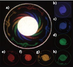
By spatially adjusting the orientation angle of rectangular holes in a 75-nm-thick chromium film, the phase modulation can be controlled across the full color range. The pixel size of the hologram is 200 × 200 nm—smaller than the wavelength of visible light and much smaller than the approximately 8 × 8 μm pixel sizes of spatial-light-modulator-based holograms—and enables a viewing angle greater than ±90°. An off-axis illumination method shifts the holographic image for different colors, overcoming crosstalk issues. For example, a seven-color holographic image of the Chinese Sun Phoenix pattern has high image quality and a 5X better signal-to-noise ratio than other meta-hologram methods. 3D holographic imaging was also realized by recording the image information into the flat meta-hologram based on a modified point-source algorithm. The high density of plasmonic pixels on the metamaterial hologram paves the way for future 3D matrix-free displays. Reference: X. Li et al., Sci. Adv., 2, 11, e1601102 (Nov. 2, 2016).

Gail Overton | Senior Editor (2004-2020)
Gail has more than 30 years of engineering, marketing, product management, and editorial experience in the photonics and optical communications industry. Before joining the staff at Laser Focus World in 2004, she held many product management and product marketing roles in the fiber-optics industry, most notably at Hughes (El Segundo, CA), GTE Labs (Waltham, MA), Corning (Corning, NY), Photon Kinetics (Beaverton, OR), and Newport Corporation (Irvine, CA). During her marketing career, Gail published articles in WDM Solutions and Sensors magazine and traveled internationally to conduct product and sales training. Gail received her BS degree in physics, with an emphasis in optics, from San Diego State University in San Diego, CA in May 1986.
