Superconducting NbN detector operates in the visible and near-infrared

Essential to progress in quantum computing is the development of single-photon photodetectors with improved properties. A group of Russian and American researchers headed by Vadim Vorobyov, who is affiliated with two Russian institutions and one Russian commercial outfit—the P.N. Lebedev Physical Institute, the Moscow Institute of Physics and Technology, and Photonic Nano-Meta Technologies LLC (all in or near Moscow, Russia)—has demonstrated a new generation of superconducting single-photon detectors (SSPDs) that have a bandwidth extending from the near-infrared (near-IR) into the visible region. Their spectral operating region of 500 to 1100 nm makes them suitable for use with leading-edge quantum emitters such as nitrogen-vacancy (NV) and silicon-vacancy centers in diamond.
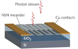
The SSPD con sists of a 4-nm-thick meandering stripe of niobium nitride (NbN) deposited on a 160 nm layer of silicon dioxide (SiO2) formed on a Si substrate. The layer of SiO2 improves photon absorption at the design wavelength range by serving as a weak broadband optical cavity. The detector has a 7 × 7 μm2 area with a 60% fill factor and is coupled to a single-mode optical fiber. It has a dynamic range of 3.5 × 10⁸ counts/s, a dark-count rate of down to 0.1 counts/s, and a jitter of 62 ps. The device can potentially be integrated on-chip with diamond emitters. The group experimentally coupled their SSPD to a 1D hyperbolic metamaterial with nanodiamond spun-coated onto it. The nanodiamonds, which were about 50 nm in size and contained NV centers, were pumped with light at a 532 nm wavelength and NV-center lifetime measured—a process assisted by the SSPD's low dark-count rate. In addition to use in quantum systems, the researchers say their detector could be useful in space-based lidar and fiber-optic sensing. Reference: V. V. Vorobyov et al., Opt. Mater. Expresshttp://dx.doi.org/10.1364/ome.7.000513 (Jan. 23, 2017).
About the Author
John Wallace
Senior Technical Editor (1998-2022)
John Wallace was with Laser Focus World for nearly 25 years, retiring in late June 2022. He obtained a bachelor's degree in mechanical engineering and physics at Rutgers University and a master's in optical engineering at the University of Rochester. Before becoming an editor, John worked as an engineer at RCA, Exxon, Eastman Kodak, and GCA Corporation.
