Semiconductor Detectors: Exotic phase of germanium could be better for IR photodetectors than ordinary Ge
Germanium (Ge) has uses in photonics by itself as a detector material, and also as a material used along with silicon (Si) to create SiGe passive and active photonics devices, including optical switches, photodetectors, and thermal imaging arrays.
An interesting area of research is the creation of forms of Ge synthesized in the lab under extreme pressure conditions. However, one of the most-promising forms of exotic Ge potentially useful for practical applications, called ST12-Ge, has only been created in tiny sample sizes—too small to definitively confirm its properties.
Conventionally formed Ge has a diamond-cubic (DC) structure at room temperature and pressure. As it is compressed, Ge changes to a metallic structure at about 10 GPa, then a body-centered orthorhombic structure at about 75 GPa, then on to a simple hexagonal structure at between 80 and 90 GPa, and finally to a hexagonal close packed (HCP) form at around 160 to 180 GPa.
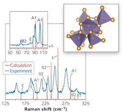
However, when compressed and then decompressed, the final state of Ge depends on the rate of decompression. To create ST12 Ge, which has 12 atoms per unit cell and is metastable, the decompression must be done slowly. The resulting ST12-Ge has a density 11% greater than DC-Ge and a complex, distorted structure made of tetrahedral elements that form rings of atoms (see figure). Rather than a discrete set of bond lengths like most crystals, ST12-Ge has a range of bond lengths and angles.
The complexity of ST12-Ge has made it hard to characterize. "Attempts to experimentally or theoretically pin down ST12-Ge's characteristics produced extremely varied results, especially in terms of its electrical conductivity," says Zhisheng Zhao, a researcher at the Carnegie Institution for Science (Washington, DC).
Zhao and his colleagues at Yanshan University (Qinhuangdao, China) and the Center for High Pressure Science and Technology Advanced Research (Pudong, China) were able to create ST12-Ge in a large-enough sample size to confirm its characteristics and useful properties. The ST12-Ge was created by putting germanium under a pressure of 14 GPa (about 1.38 × 10⁵ atmospheres) and then decompressing it slowly at room temperature.
Indirect bandgap
The millimeter-sized samples of ST12-Ge that the team created were large enough that they could be studied use spectroscopic techniques to confirm its long-debated characteristics. The researchers found that the substance is a semiconductor with an indirect bandgap of 0.59 eV and a direct optical transition at 0.74 eV.1 While direct-bandgap materials can emit light and very effectively absorb it, indirect-bandgap materials cannot.
The samples were first measured for purity using powder x-ray diffraction, along with wavelength-dispersive and energy-dispersive x-ray spectroscopy—no DC-Ge or other impurities were detected. Raman spectroscopy showed a rich Raman spectrum. Electrical-conductivity measurements at 350 K down to 150 K temperatures, along with optical absorbance and reflectivity measurements, allowed the researchers to characterize the bandgap of ST12-Ge, showing that it is a bit smaller than that for DC-Ge.
"Our team was able to quantify ST12's optical bandgap-where visible light energy can be absorbed by the material—as well as its electrical and thermal properties, which will help define its potential for practical applications," says Timothy Strobel, another Carnegie researcher. "Our findings indicate that due to the size of its bandgap, ST12-Ge may be a better material for infrared detection and imaging technology than the diamond-cubic form of the element already being used for these purposes."
REFERENCE
1. Z. Zhao et al., Nature Commun. (2017); doi:10.1038/ncomms13909.
About the Author
John Wallace
Senior Technical Editor (1998-2022)
John Wallace was with Laser Focus World for nearly 25 years, retiring in late June 2022. He obtained a bachelor's degree in mechanical engineering and physics at Rutgers University and a master's in optical engineering at the University of Rochester. Before becoming an editor, John worked as an engineer at RCA, Exxon, Eastman Kodak, and GCA Corporation.

