Single-photon Counting: Diamond-integrated single-photon detectors could lead to optical quantum circuits

Harvard University (Cambridge, MA) researchers are exploiting diamond nanophotonics—the generation, manipulation, and detection of light emitted from the defect centers of diamond—to engineer better, more broadband superconducting nanowire single-photon detectors (SNSPDs) that could be used to build integrated quantum optical circuits.1
The broad spectral transmission, wide bandgap, large Kerr nonlinearity, and high refractive index of diamond makes it an extremely attractive material for nonlinear frequency conversion, quantum information processing, and other novel nanophotonic applications.
Diamond-waveguide SNSPDs
Conventional SNSPDs consist of nanowires 4 to 8 nm thick patterned into an ultrathin film. When a wire absorbs an incident photon, the small resistive hotspot that forms generates a voltage pulse that is amplified and measured. Compared to other single-photon detectors, SNSPDs typically have better detection efficiency, lower dark count and timing jitter, and higher photon sensitivity for improved count rates.
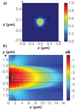
To guide the emission from diamond defect centers into the SNSPDs for direct detection, the researchers created diamond waveguides by etching free-standing triangular-shaped structures directly into diamond substrates using an angled-etching fabrication method whereby thin structures support the slightly expanded waveguide at periodic intervals. The waveguides, approximating 500-nm-sided equilateral triangles and with implanted nitrogen or silicon vacancies, channel the illumination into the SNSPDs.
Finite-difference time-domain (FDTD) simulations show that the diamond color-center fluorescence is confined in the waveguide triangular cross-section (which rejects the pump-laser illumination) and more than 99% of this fluorescence is absorbed in the first 15 μm of the SNSPD material (see figure).
Illumination of the waveguide with 705 nm light shows a wide photon-counting operational rate, and although the 4.2 K temperature and 10.5 nm superconductor thickness do not allow full saturation of the count rate of the SNSPD, the detector still remains sensitive to absorbed single photons.
"Quantum light/matter interfaces operating in the optical domain are essential to applications in quantum information processing and quantum communication," says Haig Atikian, postdoctoral scholar in applied physics at Harvard University. "Efficient generation, manipulation, and detection of photons in the realization of these systems are crucial steps to creating a truly scalable platform. With our approach it is possible to achieve monolithic and scalable integration of diamond quantum optical circuits that are based on defect color centers."
REFERENCE
1. H. A. Atikian et al., "Novel fabrication of diamond nanophotonics coupled to single-photon detectors," SPIE Newsroom (Mar. 22, 2017); https://goo.gl/goKl9M.

Gail Overton | Senior Editor (2004-2020)
Gail has more than 30 years of engineering, marketing, product management, and editorial experience in the photonics and optical communications industry. Before joining the staff at Laser Focus World in 2004, she held many product management and product marketing roles in the fiber-optics industry, most notably at Hughes (El Segundo, CA), GTE Labs (Waltham, MA), Corning (Corning, NY), Photon Kinetics (Beaverton, OR), and Newport Corporation (Irvine, CA). During her marketing career, Gail published articles in WDM Solutions and Sensors magazine and traveled internationally to conduct product and sales training. Gail received her BS degree in physics, with an emphasis in optics, from San Diego State University in San Diego, CA in May 1986.