Graphene Photonics: Low-voltage graphene electro-optic modulator operates in the near-IR

One essential component of many telecommunications-based optical systems is the electro-optical modulator, which allows the production of a stream of data using continuous-wave (CW) light as a source. Developers of leading-edge silicon (Si) photonic circuits wish to integrate these, along with compact and efficient lasers, photodetectors, and passive components, onto Si in a cost-effective way.
The complementary metal-oxide-semiconductor (CMOS) fabrication process, which is the standard in the massive Si electronics industry, allows inexpensive mass production of photonics on a Si substrate—at least if they're compatible with the CMOS process. As a result, any developer of a new photonics device who can say it's "CMOS-compatible" instantly has the ear of other developers.
Graphene is a relatively new material for photonics—it is being studied as an enabling material for various components because of its unique optical, electronic, thermal, and mechanical properties. Ideally, for cost reasons, a graphene photonic component should potentially be fabricable via the CMOS process.
A group of researchers at Manchester University (Manchester, England) has now developed an extremely small graphene-based free-space electroabsorption modulator (EAM) with a low operating voltage of 1 to 3 V and low power consumption—and it's CMOS-compatible.1
Very small modulation volume
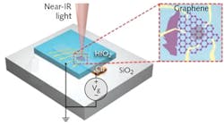
The device, which contains one high-quality graphene monolayer, acts electronically as a parallel-plate capacitor—varying the applied electrical bias varies the optical transmission of the graphene. Underneath the graphene itself is a quarter-wave dielectric hafnium dioxide (HfO2) layer with a refractive index of about 2, beneath which sits a reflective copper thin-film mirror and a quartz substrate. Electrical contacts were made to the graphene using laser-written photolithography and electron beam deposition and lift-off, producing contacts consisting of a 2-nm-thick layer of chromium and a 30-nm-thick layer of gold.
The entire device has a modulation volume on the order of 5 μm3, which could potentially be made as small as λ3 /10, the researchers say (see figure). Its power consumption is only about 1 nW, and the device's insertion loss is <10%. Broadband modulation was observed down to a wavelength of 900 nm.
The researchers note that, while capacitor-based modulators with small operational voltages had previously been developed, their modulation effects were achieved using an ionic liquid electrolyte. Solid-state dielectrics are obviously more stable, but the researchers add that solid dielectrics conventionally require high voltages of around 50 to 150 for modulation at near-IR wavelengths. It is an electrochemical supercapacitor effect observed in the HfO2 dielectric, giving it an effective capacitive thickness 10 times smaller than its physical thickness, that led to low modulation voltages of 1 to 3 V in the new device.
REFERENCE
1. D. E. Aznakayeva et al., Opt. Express (2017); https://doi.org/10.1364/oe.25.010255.

John Wallace | Senior Technical Editor (1998-2022)
John Wallace was with Laser Focus World for nearly 25 years, retiring in late June 2022. He obtained a bachelor's degree in mechanical engineering and physics at Rutgers University and a master's in optical engineering at the University of Rochester. Before becoming an editor, John worked as an engineer at RCA, Exxon, Eastman Kodak, and GCA Corporation.