Spherically curved CMOS array improves image quality across the field
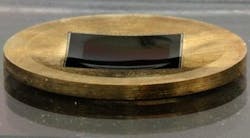
Researchers at Microsoft (Redmond, WA) and research-and-development laboratory HRL Laboratories (Malibu, CA) have figured out a way to create spherically curved CMOS sensor arrays with 3X more spherical curvature than previously reported devices. Such a spherically curved array could be used to create a camera that could image at very high quality from center to edge of the field and, at the same time, simplify the camera lens design.
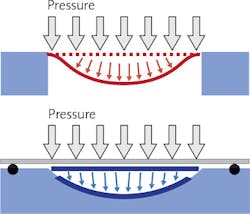
Because the process of photolithography needed to create a CMOS or CCD sensor requires the use of a very flat silicon wafer as a start, the end sensor result is also conventionally flat. But some companies have created slightly spherically curved sensor arrays by bending an already-made array to a spherical shape. These other attempts at curving a sensor have typically involved gluing the edges down and trying to push down on the center of the sensor.However, this creates points of high stress that cause the sensor to shatter before it reaches the target level of curvature. In contrast, the Microsoft researchers coaxed significantly more curvature out of the sensors by letting them float freely during the bending process, which applied pneumatic pressure and allowed stresses to dissipate gradually. They also used a specially shaped mold that very slowly builds stress around the chip's edges as it is pressed into the mold. Microsoft relied on HRL Laboratories, which has semiconductor fabrication capabilities and equipment, to help solve some of the specific physics challenges involved in bending the sensors. When used in a prototype camera with a specially designed f/1.2 lens, a curved sensor exhibited a resolution more than double that of a high-end SLR camera with a similar lens. Toward the edges of the image, the curved sensor was about 5X sharper than the SLR camera. Reference: B. Guenter et al., Opt. Express (2017); https://doi.org/10.1364/oe.25.013010.

John Wallace | Senior Technical Editor (1998-2022)
John Wallace was with Laser Focus World for nearly 25 years, retiring in late June 2022. He obtained a bachelor's degree in mechanical engineering and physics at Rutgers University and a master's in optical engineering at the University of Rochester. Before becoming an editor, John worked as an engineer at RCA, Exxon, Eastman Kodak, and GCA Corporation.

