CMOS Optoelectronics: Avalanche-mode silicon LEDs improve optical coupling in CMOS integrated circuits
In the world of silicon photonics, researchers aim to develop compact, monolithic optical platforms with integrated light sources and photodetectors to perform electronic-to-optical-to-electronic conversion at the speed of light. As with any other optoelectronic integrated circuit (IC), the goal is efficient and high-speed routing and processing of information signals on and off the chip. The same is true for complementary metal-oxide semiconductor (CMOS) platforms—however, the optical interconnect or optocoupler technology has, until now, been limited to bulky infrared (IR) sources that operate at relatively low (kilohertz) speeds.
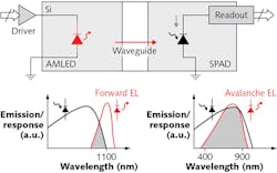
To advance optocoupling in CMOS ICs, Ph.D. student Satadal Dutta from the University of Twente (Enschede, Netherlands) has proposed using silicon (Si) light-emitting diodes (LEDs) biased in "avalanche breakdown" mode to generate visible light that is easily detected by standard Si photodiodes in a high-quantum-efficiency process.1 In addition, Dutta and PhD student Vishal Agarwal have modeled and designed a CMOS IC using avalanche-mode LEDs, waveguides, and single-photon avalanche diode (SPAD) detectors that can theoretically operate at gigahertz speeds and single-photon detection sensitivities. Essentially, the all-silicon platform avoids many of the roadblocks presented by hybrid materials systems.
All-silicon emission and detection
Current optical interconnect technology includes the use of gallium arsenide (GaAs) LEDs and Si phototransistors, providing excellent 5 kV galvanic isolation, but large (around 2 μs) delay times. Variations using III-V semiconductor materials or even organic materials can achieve 3 kV isolation, but with reported maximum speeds of only 70 kHz.2
The problem with Si interconnects has always been that the 1.12 eV indirect bandgap of Si-based light sources leads to emission at wavelengths around 1100 nm—IR emission that is essentially incompatible with Si-based photodetectors.
To improve the overlap between light-source emission and photodetection for improved quantum efficiency, Dutta focused on methods to shorten the emission wavelength of a Si-based source; namely, to operate a Si LED in avalanche breakdown mode, converting the emission to wavelengths of less than 900 nm to improve photodetection and hence, quantum efficiency (see figure). A coupling efficiency on the order of 10-9 was achieved. Dutta has shown that Si diodes with a breakdown voltage around 6 V have the highest optical power efficiency.3
Although avalanche-mode LEDs can have small-signal modulation speeds up to 20 GHz, the high bias voltages required can cause heating and parasitic effects. To address this issue, a carefully designed driver circuit using 140 nm silicon-on-insulator (SOI) CMOS technology that uses a self-quenched method to control the amount of charge fed to the LED was designed as part of the collaborative Optocoupling-in-CMOS project by Agarwal.
Finally, because avalanche-mode LEDs suffer from low (10-5) internal quantum efficiency that degrades signal-to-noise ratio (SNR), highly sensitive SPADs were the detector of choice.
Silicon waveguiding
In between the source and detector is a crucial link in all-silicon IC design: the waveguide, which is the most-challenging part in the whole design because of limited options. Dutta says, "Guiding photons in contemporary silicon-on-insulator [SOI] technology is as effective as distributing water via a leaky, mud-clogged pipeline. One needs to resort to other dielectric films in the CMOS layer stack to transport visible light."
A combination of SOI and a CMOS-compatible dielectric such as silicon nitride (Si3N4) can propagate both the visible and the near-IR spectrum of light laterally within the chip over distances of more than 10 μm. Finite-difference time-domain (FDTD) simulations were used to study the decisive geometrical factors for the waveguide efficiency in conjunction with the broad-spectrum and isotropic LED emission characteristics.
"Avalanche-mode Si LEDs are very rich in their potential and underlying physics," adds Dutta. "Many mysteries are yet to be solved, but it is overwhelming that the simplest semiconductor device—a p-n junction—can emit such a broad and fluid spectrum of light depending on the device design and the technology."
REFERENCES
1. S. Dutta, "Avalanche-mode silicon LEDs for monolithic optical coupling in CMOS technology," PhD Thesis, University of Twente (Nov. 8, 2017); see https://ris.utwente.nl/ws/portalfiles/portal/17337861.
2. D. Li et al., IEEE Electron. Device Lett., 36, 2, 171–173 (2015).
3. S. Dutta et al., IEEE Electron. Device Lett., 38, 7, 898–901 (2017).

Gail Overton | Senior Editor (2004-2020)
Gail has more than 30 years of engineering, marketing, product management, and editorial experience in the photonics and optical communications industry. Before joining the staff at Laser Focus World in 2004, she held many product management and product marketing roles in the fiber-optics industry, most notably at Hughes (El Segundo, CA), GTE Labs (Waltham, MA), Corning (Corning, NY), Photon Kinetics (Beaverton, OR), and Newport Corporation (Irvine, CA). During her marketing career, Gail published articles in WDM Solutions and Sensors magazine and traveled internationally to conduct product and sales training. Gail received her BS degree in physics, with an emphasis in optics, from San Diego State University in San Diego, CA in May 1986.
