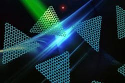
Room-temperature boron nitride monolayer light source emits single photons on demand
Many advances in quantum-optical technology are highlighted in Laser Focus World, including photon sources, detectors, and optical and fiber-optics systems that maintain entanglement between photons. The topic of quantum optics may seem esoteric, but it has the potential to produce powerful results, such as truly secure communications, and quantum computers that have the ability to solve hugely complex problems—such as deciphering just about any type of encrypted communications that is not quantum-based.
Along these lines, researchers at the University of Technology Sydney (UTS; Ultimo, Australia) have created a type of single-photon emitter that both operates at room temperature and is two-dimensional (unlike previous bulky 3D devices), meaning that it can be integrated into photonic chips.1 Based on a molecular monolayer of hexagonal boron nitride containing a color center, the light source produces polarized single-photon emission on demand, useful for quantum information processing.
Igor Aharonovich, one of the UTS researchers, says the single photon sources are brighter than any other others currently available and are promising enablers for absolutely secure communications and quantum computation.
"This material is very easy to fabricate," says Trong Toan Tran, another UTS researcher. "It's a much more viable option because it can be used at room temperature; it's cheap, sustainable and is available in large quantities. "Ultimately we want to build a 'plug and play' device that can generate single photons on demand, which will be used as a first prototype source for scalable quantum technologies that will pave the way to quantum computing with hexagonal boron nitride."
Source: http://newsroom.uts.edu.au/news/2015/10/quantum-communications-go-thin-and-light
REFERENCE:
1. Toan Trong Tran et al., Nature Nanotechnology (2015); doi: 10.1038/nnano.2015.242

John Wallace | Senior Technical Editor (1998-2022)
John Wallace was with Laser Focus World for nearly 25 years, retiring in late June 2022. He obtained a bachelor's degree in mechanical engineering and physics at Rutgers University and a master's in optical engineering at the University of Rochester. Before becoming an editor, John worked as an engineer at RCA, Exxon, Eastman Kodak, and GCA Corporation.
