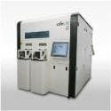
Starnberg, Germany - Rofin-BAASEL Lasertech has entered the semiconductor market with a turnkey solution for front-end-of-line (FEOL) processing. The new laser wafer processing system, Waferlase 200/300/450, is a fully automated modular platform comprising a handling system for (ultra) thin semiconductor wafers and a choice of laser processing modules, depending on the type of application. The Waferlase 200/300/450 product family has solutions for IGBT laser annealing and debris-free wafer marking.
Rofin's integrated wafer handling technology provides precise, non-contact transportation of ultra-thin wafers, even with considerable warpage and bow. The system comes with two or more cassette ports for Open Cassette or FOUP wafer carrier systems. Integrated scanners detect the exact position of the wafer in its carrier. The comprehensive but easy-to-use system software controls slot allocation, wafer warpage measurement, wafer location as well as wafer ID detection, and would even change the pick-and-place sequence automatically in case of a wafer damage threat, e.g. due to extensive or opposite bowing of neighboring wafers. A high-end dual-arm robot takes care of wafer loading and unloading. The pre-aligner module centers and aligns the wafer. A “vacuum handshake” between end-effector and pre-aligner, including wafer safeguard, secures damage-free handling of the wafer back side.
Rofin’s Waferlase 200/300/450 systems produce traceable markings on transparent, semitransparent, and opaque wafer materials. Two methods - hard and debris-free marking - are used that differ in terms of process, depth and location of the mark. Debris-free marking in a cleanroom environment is achieved solely by melting of the silicon wafer surface. Rofin's new patent-pending marking technology allows the user to precisely control the marking depth ranging from less than 1 to 7 micron. The debris-free marking process uses a tailor-made IC-marking laser source with 532 nm wavelength.
