Assembly solution addresses TO-can photonic device manufacturing challenges
The next generation of mobile Internet connectivity will rely on deployment of 5G networks, which promise to supercharge Internet of Things (IoT) technology with the powerful communication infrastructure needed to carry vast amounts of data. While the transition and upgrade to 5G will allow for a smarter and more connected world, it will also require a huge investment to cope with expected growth in network costs.
To this effect, 5G network deployment not only increases demand for high-speed and low-power consumption photonics devices, but also increases cost pressures on such devices. The number of optical devices built and sold grows at approximately 25% per year, but the price of the devices decreases at a rate greater than 10% per year. Consequently, a low-cost solution for the automated assembly of 5G high-performance photonics devices is becoming a priority for photonic device manufacturers.
TO-can package
The common transistor-outline-can (TO-can) package for optical components is an industry standard that governs the design and size of current-conducting microelectronic packaging and housings. Having been used for several decades, a TO package always consists of two components: a TO header and a TO cap. While the TO header ensures that the encapsulated components are provided with power, the cap ensures the smooth transmission of optical signals.
Since the package is a major materials cost factor for photonic devices, the aim of many recent developments covers various kinds of low-cost packaging designs for high-performance optical devices. These innovative design activities drive continued cost reductions. In recent years, many improved TO-can package designs for different optical applications have been developed.
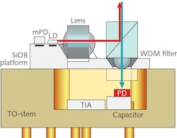
In 2013, the Electronics and Telecommunications Research Institute in Korea published an article explaining a new, low-cost bidirectional optical subassembly (BOSA) that uses a single glass-sealed conventional TO-can package for the passive optical network application (see Fig. 1). This BOSA incorporates optical transmitting and receiving functions into a silicon optical bench and in a TO-can package, providing a low-cost BOSA for 10 G-EPON and XG-PON applications.1
In 2015, Lightip launched a TO‐can-based tunable laser transmitter optical subassembly (TOSA) at OFC, which is based on an 8-pin TO-can package that offers cost reduction. The compact and low-cost tunable laser has up to 16 channels at 100 GHz spacing or up to 32 channels at 50 GHz spacing especially suited for NGPON2 and wavelength-division multiplexing (WDM)-PON.
At the OFC conference in 2018, Bernhard Schrenk from the AIT Austrian Institute of Technology and Fotini Karinou from Huawei Technologies Duesseldorf GmbH published the “World’s First TO-can Coherent Transceiver.” They achieved the coherent homodyne receiver and transmitter in a TO-can package with a single fiber/RF port.2
In the same year, Sae-Kyoung Kang and their team designed and implemented a cost-effective and compact 100 Gbit/s (2 × 50 Gbit/s) PAM-4 receiver optical subassembly (ROSA) by using a TO-can package instead of an expensive box-type package. It consists of an optical demultiplexer, two PIN-PDs, and a 2-channel linear transimpedance amplifier. The components are passively aligned and assembled using alignment marks engraved on each part.3
Today, the new TO-can packages have more complex functions beyond the traditional low-cost simple transmitters and receivers in traditional optical transponders, such as cooled/uncooled 50G DML/EML transmitters, tunable lasers, BOSAs, 980 pump lasers, and 100G PAM4 receivers.
While those high-performance or complex functions were formerly packaged in the complex expensive box-type packages, now the focus of these new TO-can photonic devices with new technology and high performance is to reduce costs and package size. However, it is quite difficult to integrate the active transmitting and receiving components with the passive waveguide, optical filter, and other components partly or simultaneously in the same exceedingly small TO-header.
Furthermore, these new low-cost TO-can photonic devices are deployed in high-volume application scenarios. During OFC 2018, TO-can package supplier Schott introduced 50G TO-can packages, which represents the start of a new chapter in the development of ultra-high-speed technology that make deploying the most capable networks possible and satisfying ever-increasing deployment demand. Such devices support up to 400G with QSFP transceivers in datacenter interconnect (DCI) and enable faster data transmission to wireless stations to help the telecom industry make the step towards deploying 5G cellular networks.
To support 5G wireless deployment, WDM lasers and electro-absorption modulated lasers (EMLs) are packaged into low-cost TO-can packaging. With multi-dies requiring attachment, these WDM/EML-TOs are far more complicated than traditional TO-can packaging that only need to handle 1–2 dies.4
Both DCI and 5G applications have high volume demands and are extremely cost-sensitive with stringent requirements for manufacturability. If there is no cost-effective fully automated solution for the new TO-can photonic device, such new devices may not be able to meet cost targets, critical for widespread commercial applications.
Challenges of assembly automation
Different size TO-Can packages selected for new photonic devices to achieve multiple functions, such as TOSA, ROSA, tunable laser, and transceivers are packaged as TO-38 or TO-56. The chip materials can be a III-V compound semiconductor for transmitting and receiving chips, together with other dies, like TEC, glass lens, filter, isolator, TIA, and other optical or electrical components. All of these components will be attached in a small TO header.
The process may include eutectic, epoxy, and UV cure. These chips/dies may be designed horizontal or vertical or even with some angle for attaching in the customized new TO header. Assembly solutions typically replace active alignment, which is expensive and has longer cycle times, with low-cost passive alignment that uses alignment marks engraved on each part.
This challenge requires a multi-process, high-accuracy, fully automated machine to support volume manufacturing of different types of new TO-can devices because optical components such as photodiodes, laser diodes, and lenses in the new TO-can packages are particularly susceptible to small assembly tolerances, especially for single-mode designs.
For the optical parts’ passive alignment, the higher-accuracy placement is necessary for optical chips/dies. In the new TO packaging design, the chips/dies position tolerance may need less than ±3–5 µm; this requires the machine to have higher-accuracy ±1~2 µm. Greater machine accuracy releases more tolerance to the components, which may, in turn, reduce the materials cost and increase assembly yield in volume manufacturing.
Another challenge is to have the flexibility to quickly handle various types of TO headers. The new TO header has different direction alignment marks to make sure the multiple components can be mounted in the TO header properly. A solution is needed to handle the new TO header with multiple leads with lead lengths of 14 to 18 mm. The TO header may require pre-positioning to rotate the TO header in the right position.
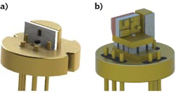
In general, such TO headers use a mark, small pin, cavities, or special structures on the TO header for alignment, with cavities and special structures more popular in the new 5G TO headers (see Fig. 2). After pre-positioning for the TO-header, the bonding station must be designed to fit the TO-can package, as must the TO-header eutectic heating station. The machine should also be easy to program or reconfigurable to fit in a different TO header size.A third challenge is that new TO-can packages have multiple chips/dies in a small TO header. Usually, there are at least two to six different optical and electrical components in a new TO-header, and in some instances greater than six. The chips/dies may use different materials and have different sizes, as well as use a different bonding process such as eutectic or epoxy.
The die bonder machine needs the capability to quickly change the pick-and-place tools to handle these materials. The chip/die materials may be required to have different input modes, such as wafer, waffle pack, or Gel-Pak. By supporting these different bonding processes within a single machine, additional calibration errors between bonding machines can be avoided and high accuracy achieved.
Another challenge is that the new TO-photonic devices must be produced at high volumes to achieve low cost. The fully automated solution needs very high efficiency with minimal process cycle times. Achieving this requires that the machine be designed for high-speed and parallel processing to meet the customer’s throughput requirements.
At the same time, the machine must have the flexibility to handle a variety of new TO-Can package devices, with the capability to easily change fixtures and have easy programming to switch from one product to another. One TO machine can be considered as one TO-can device assembling unit in an FMS (Flexible Manufacturing System).
Innovative solution and results
Understanding these challenges, engineers at MRSI Systems (Tewksbury, MA) have developed a fully automated assembly solution for volume manufacturing of the new TO-can packages. Dubbed MRSI-H-TO, the machine is built based upon the company’s next-generation, 1.5 µm accuracy, flexible high-speed die bonder platform5 for multi-dies and multiple processes.
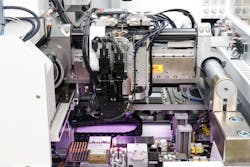
Targeting the new TO-can photonic devices volume manufacturing for the high-speed DCI and 5G wireless network rollout, MRSI-H-TO adopts 50 nm resolution linear motor and an air-bearing gantry for precision movement in XYZ directions. The machine ϴ can have 360° travel with 0.0045° resolution, and its placement accuracy can meet ±1.5 µm without rotation and placement repeatability can be within ±1 µm @ 3 sigma (see Fig. 3).The TO handler module also has one TO pre-positioning stage to rotate the TO header to the right position—which may not be needed for some TO with clear orientation features—by recognizing the TO header direction alignment mark. This TO handler module with rotational dual ultrafast ramp eutectic stages can provide parallel processing between loading/unloading and eutectic bonding.
The TO handler module can handle multiple sizes of TO such as TO 38/46/56/65/72. The result is maximum throughput while maintaining flexibility for tool changes.
This system that can be configured with an ultrafast-ramp eutectic station, parallel material handling, and dual bonding stages, and provides the unique capability of handling and bonding multiple-dies of distinct size and geometry without machine changeover.
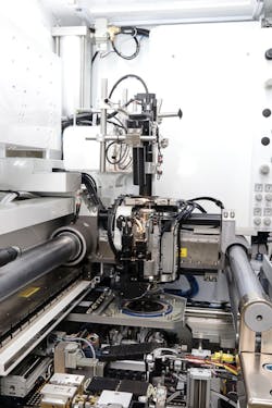
A real-time force control bonding head with programmability from 10 to 300 grams of force can handle the minimum die size of 140 µm. The gantry bonding head with an “on-the-fly” tool changer has ±1.5 µm die placement accuracy to complete both eutectic and epoxy stamping bonding. Material input options include wafer, waffle pack, and Gel-Pak (see Fig. 5).Formerly, dealing with this wide range of challenges would require investing in two different machines, which would be expensive and inefficient, leading to longer total process time and thus lower throughput. Perhaps worst of all, the final post-process accuracy was weak, as the deployment of two machines compounded calibration errors.
In some cases, this led to the original center of the TO-base being unrecognizable for the second machine after it was covered by some dies bonded by the first machine. MRSI’s innovative solution for the multi-die and multi-process benefits customers with best-in-class throughput for capacity expansion, high accuracy for advanced high-density product packaging, and unmatched flexibility for any kind of TO-can photonic device production in one machine, thus transforming the economics and accuracy of the die bonding process.
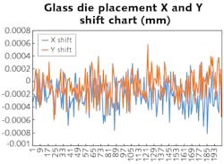
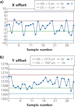
A customer site experiment building 25G DML TO56 for 5G TOSA involved a 90° flip-chip eutectic die bonding process, and a total of 29 pieces of 25G DML TO56 products were built. X and Y offset results (see Fig. 6) are well within product specifications with post-bonding both X accuracy and Y accuracy within ±5 µm @3 sigma. The machine also demonstrated industry-leading speed and total throughput for the complex TO products in handling multi-die and multi-processes.Summary
The low-cost TO-can package is starting to be used for high-performance photonics devices, which is driven by the DCI and 5G rollout. The new TO-can package is far more challenging than the traditional TO-can package, requiring higher accuracy with multi-dies and multi-processes within one machine for the high-mix and high-volume manufacturing of the high-performance photonic devices.
MRSI-H-TO provides an innovative solution to address the manufacturing challenges for the new TO photonic devices. The field test results demonstrated the post-bonding accuracy in a high-volume environment for multi-die and multi-process TO-based devices. This is the first fully automated machine in the world to meet the new TO-can high-accuracy, high-speed, high-flexibility requirements.
ACKNOWLEDGEMENT
Gel-Pak is a registered trademark of Gel-Pak, a division of Delphon Industries.
REFERENCES
1. Y. S. Heo et al., Opt. Eng., 52, 1 (Jan. 2013).
2. B. Schrenk and F. Karinou, OSA Technical Digest (online), paper Th1A.4 (2018).
3. S.-K. Kang et al., Opt. Express, 26, 5, 6172 (Mar. 2018).
4. Y. Qian, “Manufacturing Photonics: Challenges for photonics manufacturing in the new data center era,” Laser Focus World, 54, 8, 24–29 (Aug. 2018); https://bit.ly/MRSIRef4.
5. L. Zhou, “Flexible die bonding solution targets modern photonics manufacturing,” Laser Focus World, 56, 7, 35–37 (Jul. 2020); https://bit.ly/MRSIRef5.
Limin Zhou | Senior Director of Strategic Marketing, MRSI (Mycronic Group)
Dr. Limin Zhou is senior director of strategic marketing at MRSI Systems (Mycronic Group), Tewksbury, MA.
