One of the biggest challenges facing manufacturers of smartphones, consumer electronics, and augmented-reality/virtual-reality/mixed-reality (AR/VR/MR) devices is component miniaturization. The need to create smaller, lighter, and more compact devices continues to grow, while simultaneously making performance gains..
A metalens is a flat optics technology with metasurfaces to bend and steer the light, and metalenses are swiftly emerging as a promising solution to meet this need. Indeed, entire conferences are now dedicated to the topic because meta-optics is recognized as a pioneering technology with massive commercial potential. It can disrupt numerous applications, such as simplified time-of-flight (ToF) systems; ultracompact near-infrared (NIR) cameras used for eye-tracking and driver monitoring; sensing and machine-vision applications; shortwave-infrared (SWIR) imaging to detect food freshness and food contamination; medical imaging; lidar; presence detection within smart homes; object detection/avoidance in robotics; and health/biometric sensing. The list is long and continues to grow.
With metalenses, lens systems in optical applications can be significantly reduced in size and complexity by replacing refractive lens elements with metalenses. The reduction of elements in optical systems brings a variety of benefits: easier assembly, increased functionality of optical applications, higher efficiency, and significantly better imaging quality.
It’s one thing, however, to demonstrate high efficiency of metalenses and explain how optical systems can be optimized by substituting refractive lenses. It’s quite another to design, develop, and mass-manufacture such leading-edge technology. The challenge is figuring out how to manufacture more breakthrough optical solutions at scale for widespread commercialization.
To do this, several hurdles need to be addressed. On the market side, product managers want to understand the pros and cons of the new technology, its price/performance advantages, and what new features or capabilities it provides. On the technology side, cutting-edge technology companies want to focus their efforts on areas relevant to the markets and investments that can be monetized rapidly.
Entering fast prototyping provides an efficient and low-risk way to quickly discover what the market wants and what a new technology can deliver. In today’s ever-more complex optics systems, changing a lens element from a refractive solution to a diffractive one may change how the modules are assembled, how the software application using the camera module is fine-tuned, and even how camera sensors are optimized for best system performance. While requirements, talks, and simulations can help, product architects want prototypes that can be put through a real-world use case to see how the entire system responds.
Mass production of meta-optics
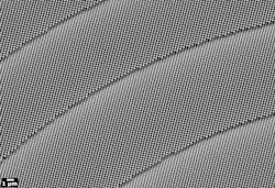
The Danish optical solutions company NIL Technology (NILT) develops and mass-produces meta-optics for smartphones, consumer electronics, and AR/VR/MR. Depending on the application, NILT’s meta-optical elements (MOEs) are comprised of arrays of pillars to sub-100 nm diameters with vertical sidewalls (see Fig. 1).
These pillars require tolerances of less than a few nanometers to achieve high-efficiency optics performance. Instead of the curved surface of a traditional refractive lens element, MOEs are entirely flat, but effectively create the same result. They bend and redirect the light, using a single MOE in place of several lenses stacked on top of each other. The MOE itself is made in silicon on a glass substrate, making it strong, rigid, reliable, and thermally stable. It can be customized for wavelengths in visible, NIR, and SWIR bands.
Because of the subwavelength lateral size of nanostructures, most metasurfaces demonstrated by academic institutions are fabricated with e-beam lithography (EBL). EBL is a high-resolution, high-fidelity technology, however ill-suited as a standalone for commercial purposes, due to the time-consuming rasterization of the electron beam.
But when combined with nanoimprint lithography (NIL), EBL provides the possibility of fabricating high-quality, low-cost MOEs in batch sizes suitable for mass production. This is enabled by using mechanical deformation of imprint resist to create copies of the initial EBL-written master.
Making a NIL replica using an EBL master secures high design freedom and low-cost prototyping. It provides a significantly quicker turnaround time than deep-UV lithography (DUV), which requires the fabrication of a new mask when a design parameter is changed. At the end of 2021, extensive experience in EBL and NIL, combined with sophisticated optical design methods and advanced in-house optical characterization, allowed NILT to introduce a single-surface metalens with an unprecedented absolute efficiency of 94% (see Fig. 2).While most of the work in MOEs within the past 20 years was concentrated in academia, NILT is now commercializing their MOE technology by structuring all processes for mass production. NILT’s first focus is 3D sensing for mobile phones on both the front- and world-facing sides, but the technology has the potential to disrupt numerous applications.
Sensors are everywhere today, and tend to have common problems in weight, size, performance, and efficiency. A wide range of applications can benefit from the mass production of MOEs, which can eliminate the number of elements required in optics systems, will be easier to assemble, and provide far more functionality. All in all, MOEs finally make it possible to rethink how an optical system is made and harvest the benefits of a significantly simpler, smaller, and better-performing system.
Thorlak Vestergaard | VP Manufacturing & Technology, NIL Technology (NILT)
Thorlak Vestergaard has worked with manufacturing, supply chain, and operations management in industry-leading global high-tech companies for more than 20 years. His primary experience stems from bringing mobile phones into production for Nokia Mobile Phones and managing the supply chain and operations for Jabra (part of GN Audio A/S, Denmark).
Since mid-2020, Thorlak has been with NIL Technology (NILT; Kongens Lyngby, Denmark), an optical solutions company within diffractive optics and meta-optics. His mission is to bring the precision of E-beam lithography into mass manufacturing of high-performing optical elements for sensing applications.


