MICRO-OPTICS FABRICATION: 3D microfluidic mask method rapidly fabricates microlenses
Microlenses and microlens arrays can be fabricated using a myriad of methods such as ultraviolet (UV) molding, hot embossing, photoresist and electron-beam lithography, and microjet fabrication. Unfortunately, some of these micro-optics fabrication methods require complex molds and none enable dynamic adjustment of microlens parameters. But a new three-dimensional (3D) microfluidic method from researchers at National Taiwan Ocean University (Keelung, Taiwan) and Mingchi University of Technology (Taipei, Taiwan) is removing these obstacles.1 Not only does the method allow rapid and low-cost fabrication without molds or complex illumination optics, it also enables dynamic parameter changes for microlenses or microlens arrays during the continuous-fabrication process.
A single-step process
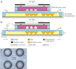
The continuous, high-throughput fabrication process comprises two main components: first, an electrostatic-force-modulated (EFM)-3D gray mask; and second, an all-polydimethylsiloxane (PDMS) microchannel (see figure). The EFM-3D gray mask consists of a flexible, transparent elastomer structure filled with index-matching oil that contains UV-light-absorbing dies to provide the desired attenuation factor for the input illumination. A rectangular PDMS microchannel is then bonded onto a glass slide coated with a thin PDMS film. Indium tin oxide (ITO) glass on the top and bottom of the structure conducts to create the electrostatic forces required to deform the elastomer structures in the vertical direction. Finally, a shadow mask placed on top of the EFM-3D gray mask defines the dimensions of the microlens or microlens array.
To fabricate a micro-optic structure, an HDDA acrylate containing a photosensitive initiator is pumped into the microchannel structure. Voltage is applied to the ITO layers until the desired semicircular or aspherical shape is approached for the EFM-3D gray mask. Illumination is then applied, resulting in the transfer of the desired gradient distribution profile into the HDDA acrylate—polymerizing it in less than one second and creating a microlens or array per the design goals.
The polymerized micro-optic structures then flow downstream without adhering to the microchannel surfaces due to an oxygen-aided inhibition layer on the PDMS surfaces. The inhibition layer arises from the diffusion of molecular oxygen through the PDMS surface that reacts with an initiator to form an unpolymerized lubrication layer approximately 3 μm thick.
Dynamic fabrication
To change the structural dimensions of the resultant microlenses or arrays, either the concentration of UV-light-absorbing dyes in the refractive-index oil can be altered, or the applied voltage can be varied. Either or both of these changes in turn alters the intensity distribution of the light passing through the 3D gray mask, changing the shape of the structures.
Using OSLO optical simulation software from Lambda Research (Littleton, MA), the shapes of some fabricated microlenses were compared to the light-intensity distribution profiles applied during the fabrication process. The analysis showed that selection of both refractive-index oil and dye concentration, as well as applied voltage, figured heavily into accurate predictions of lens shape.
Shih-Hao Huang, an assistant professor at National Taiwan Ocean University, says, "Because the microlens arrays are allowed to flow downstream without problematic adhesion to the sidewalls for continuously high-throughput production, there are ongoing efforts to perform the microfluidic self-assembly of the produced microsize microlens arrays into the centimeter scale of a microlens-based diffuser. For this targeted commercial application in the display industry, the microlens-based diffuser could be used in liquid-crystal displays or digital micromirror device (DMD) projectors to improve the brightness and uniformity of the illumination light on the whole screen."
REFERENCE
1. S.-H. Huang et al., SPIE J. Micro/Nanolithography MOEMS MEMS, 9, 4, 043002-1 to 043002-9 (Dec. 7, 2010).

Gail Overton | Senior Editor (2004-2020)
Gail has more than 30 years of engineering, marketing, product management, and editorial experience in the photonics and optical communications industry. Before joining the staff at Laser Focus World in 2004, she held many product management and product marketing roles in the fiber-optics industry, most notably at Hughes (El Segundo, CA), GTE Labs (Waltham, MA), Corning (Corning, NY), Photon Kinetics (Beaverton, OR), and Newport Corporation (Irvine, CA). During her marketing career, Gail published articles in WDM Solutions and Sensors magazine and traveled internationally to conduct product and sales training. Gail received her BS degree in physics, with an emphasis in optics, from San Diego State University in San Diego, CA in May 1986.
