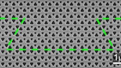
Engineers at Duke University (Durham, NC) have demonstrated a photonic-crystal (PhC)-based device that can direct photons around sharp corners with virtually no losses due to backscattering, a key property that will be needed if electronics are ever to be replaced by photonic devices.1 The result was achieved with PhCs built on the concept of topological insulators.
By carefully controlling the geometry of a crystal lattice, researchers can block light from traveling through its interior while transmitting it perfectly along its surface. The device accomplishes its near-perfect transmittance around corners despite being much smaller than previous designs. "The smaller the device the better, but of course we're trying to minimize losses as well," says Wiktor Walasik, a postdoctoral associate in electrical and computer engineering at Duke. "There are a lot of people working to make an all-optical computing system possible. We’re not there yet, but I think that’s the direction we're going."
Previous demonstrations have also shown small losses while guiding photons around corners, but the new Duke research does it on a rectangular device just 35 µm long and 5.5 µm wide, which is 100 times smaller than for previously demonstrated ring-resonator-based devices. In the new study, researchers fabricated optical topological insulators using electron-beam lithography and measured the light transmittance through a series of sharp turns. Each turn only resulted in the loss of a few percent.
"Guiding light around sharp corners in conventional photonic crystals was possible before but only through a long laborious process tailored to a specific set of parameters," says Natasha Litchinitser, a professor of electrical and computer engineering at Duke. "And if you made even the tiniest mistake in its fabrication, it lost a lot of the properties you were trying to optimize."
The researchers point out that their device also has a large operating bandwidth, is compatible with modern semiconductor fabrication technologies, and works at wavelengths currently used in telecommunications. Now the researchers are trying to make a waveguide that can be switched on or off at will.
Source: https://pratt.duke.edu/about/news/optical-waveguide
REFERENCE:
1. Mikhail I. Shalaev et al., Nature Nanotechnology (12 November, 2018); doi: 10.1038/s41565-018-0297-6.

John Wallace | Senior Technical Editor (1998-2022)
John Wallace was with Laser Focus World for nearly 25 years, retiring in late June 2022. He obtained a bachelor's degree in mechanical engineering and physics at Rutgers University and a master's in optical engineering at the University of Rochester. Before becoming an editor, John worked as an engineer at RCA, Exxon, Eastman Kodak, and GCA Corporation.
