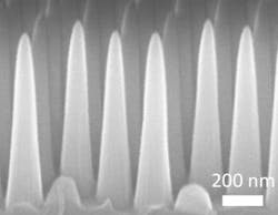
MIT researchers create nanostructured surface for glass that is antireflection, hydrophobic, and antifogging
Cambridge, MA--A surface nanostructure that is photolithographically etched onto glass by scientists at the Massachusetts Institute of technology (MIT) gives the glass both water repellancy and antireflection qualities.1
The new “multifunctional” glass, based on surface textures that consist of arrays of nanosized cones that are 200 nm wide and 1 micron tall, is self-cleaning and resists fogging and glare, the researchers say. Ultimately, they hope it can be made using an inexpensive manufacturing process that could be applied to optical devices, the screens of smartphones and televisions, solar panels, car windshields, and windows in buildings.
Although the arrays of pointed nanocones on the surface appear fragile when viewed microscopically, the researchers say their calculations show they should be resistant to a wide range of forces, ranging from impact by raindrops in a strong downpour or wind-driven pollen and grit to direct poking with a finger. Further testing will be needed to demonstrate how well the nanotextured surfaces hold up over time in practical applications.
Fabrication begins by coating a glass surface with several thin layers, including a photoresist layer, which is then illuminated with a grid pattern and etched away; successive etchings produce the conical shapes. The team has already applied for a patent on the process. Because it is the shape of the nanotextured surface, rather than any particular method of achieving that shape, that provides the unique characteristics, in the future glass or transparent polymer films might be manufactured with such surface features by passing them through a pair of textured rollers while still partially molten; such a process would add minimally to the cost of manufacture.
Photovoltaic panels, explains Kyoo-Chul Park, one of the researchers, can lose as much as 40% of their efficiency within six months as dust and dirt accumulate on their surfaces. But a solar panel protected by the new self-cleaning glass, he says, would have much less of a problem. In addition, the panel would be more efficient due to the surface's antireflection qualities.
While some earlier work has treated solar panels with hydrophobic coatings, the new multifunctional surfaces created by the MIT team are even more effective at repelling water, keeping the panels clean longer, the researchers say. In addition, existing hydrophobic coatings do not prevent reflective losses. Other applications could include optical devices such as microscopes and cameras to be used in humid environments, where both the antireflective and anti-fogging capabilities could be useful. In touch-screen devices, the glass would not only eliminate reflections, but would also resist contamination by sweat.
REFERENCE:
1. Kyoo-Chui Park et al., ACS Nano, pub. date (Web): April 8, 2012; DOI: 10.1021/nn301112t

John Wallace | Senior Technical Editor (1998-2022)
John Wallace was with Laser Focus World for nearly 25 years, retiring in late June 2022. He obtained a bachelor's degree in mechanical engineering and physics at Rutgers University and a master's in optical engineering at the University of Rochester. Before becoming an editor, John worked as an engineer at RCA, Exxon, Eastman Kodak, and GCA Corporation.
