Cornell CMOS-compatible mid-IR optical frequency comb fits on 1 mm chip
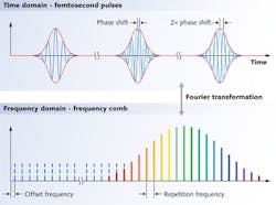
Researchers at Cornell University (Ithaca, NY) have miniaturized an optical frequency comb light source emitting in the elusive mid-infrared (mid-IR) spectrum, effectively squeezing the capabilities of a large tabletop laser onto a 1 mm silicon chip.1 The device could lead to highly sensitive handheld gas sensors for anything from atmospheric research to disaster-recovery missions. The CMOS-compatible miniature frequency comb, which spans from 2.1 to 3.5 μm, hails jointly from the Cornell labs of Michal Lipson and Alexander Gaeta.
Aiming at the fingerprint region
Mid-IR frequency combs are of widespread interest for gas sensing applications, because in this wavelength (the so-called fingerprint region), many different gases have strong spectral absorption lines. Engineers want to exploit this wavelength range for sensitive detection of a large array of gases.
The Cornell researchers fabricated the silicon structure with a thermal oxidation process that makes surfaces very smooth, leading to reduced optical losses compared with conventional silicon optics. They also solved the problem of silicon building up too much charge at high optical powers by placing a diode on the device that swept out built-up electrical charges so that the light source was not affected by the few charges that were left.
The experiments were carried out by first author Austin Griffith, a graduate student in Lipson's lab. The devices were fabricated at the National Science Foundation-supported Cornell NanoScale Science and Technology Facility. The research was supported by the Defense Advanced Research Projects Agency and the Air Force Office of Scientific Research.
Source: http://www.news.cornell.edu/stories/2015/02/precision-gas-sensor-could-fit-chip
REFERENCE:
1. Austin G. Griffith et al., Nature Communications (2015); doi:10.1038/ncomms7299

John Wallace | Senior Technical Editor (1998-2022)
John Wallace was with Laser Focus World for nearly 25 years, retiring in late June 2022. He obtained a bachelor's degree in mechanical engineering and physics at Rutgers University and a master's in optical engineering at the University of Rochester. Before becoming an editor, John worked as an engineer at RCA, Exxon, Eastman Kodak, and GCA Corporation.
