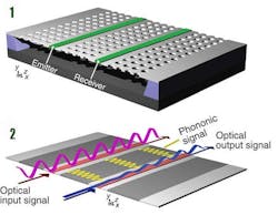
| Two green silicon optical waveguides are shown embedded in a gray photonic crystal membrane (top). In the bottom image, the violet and blue curves represent optical input and output signals; the yellow curves represent transduced phonon waves. (Image: Sandia National Laboratories) |
Scientists from Yale University (New Haven, CT), Sandia National Laboratories, (Albuquerque, NM), and the University of Texas at Austin have built a device that, by coupling laser photons with phonons (vibration quanta), allows an integrated silicon photonic circuit to do efficient signal processing of radio-frequency (RF) info such as radar data.1
Because phonons travel at the speed of sound rather than light, the slower velocity allows data to be stored, filtered, and delayed over very small length scales with high fidelity. The RF filters would form the basis for spectrometers that would let users “see” energies placed in various frequency bands across a wide spectral range.
The novel, very thin filter structures are in the laboratory stage. A system demonstration, complete with lasers, modulators, detectors and battery, should be a bit larger than a computer hard drive, weigh only a few pounds, and become available within three to five years.
Using the nano-optomechanical coupling approach, the researchers were able to combine the high bandwidth offered by light (demonstrated at frequencies up to 20 GHz and easily extended to 100 GHz) with the linearity and sharp resonances provided by phononic filters. The energy cost of this photon-to-phonon conversion is offset by the high-resolution filter responses that exhibit very little signal distortion over a wide frequency range, says Charles Reinke, who leads the effort at Sandia National Laboratories.
Creating a phononic crystal requires taking a thin film of material, in this case silicon nitride (SiN), and modifying its mechanical properties via the phononic-crystal lattice. For the filtering system, two materials are key: SiN to form the membranes in which the acoustic signals propagate, and silicon to form optical waveguides. The dual system optimizes the acoustic and optical properties of the device independent of each other.
The photonic-phononic devices also could be incorporated with on-chip photodetectors and other electronics.
The work was initiated by Sandia's Laboratory Directed Research and Development office and is currently funded for almost $5 million by the Defense Advanced Research Projects Agency (DARPA).
Source: https://share.sandia.gov/news/resources/news_releases/phononic_filter/
REFERENCE:
1. Heedeuk Shin et al., Nature Communications (2015); doi: 10.1038/ncomms7427
