CCD/CMOS Sensors: CMOS has come a long way for imaging in life sciences
RACHIT MOHINDRA
An examination of how sensor technologies have progressed in the low-light imaging arena shows how recent changes in technology have raised the bar for current industry standards in the realm of scientific imaging. These changes will have an impact in the lab.
Depending on the image sensor used, scientific cameras are termed charge-coupled devices (CCDs), electron-multiplying CCDs (EMCCDs), or scientific complementary metal-oxide semiconductor (sCMOS) devices. Microscopy cameras are engineered with these important considerations:
Resolution: matching the camera resolution to the microscope resolution and sample feature.
Speed: keeping pace with transient phenomena while preserving requisite sensitivity.
Sensitivity: optimizing detection of wavelengths of interest, minimizing living cells' exposure to bleaching effects and toxicity of illumination energy.
Automation: streamlining the operation of camera system as part of a complex experimental apparatus.
Triggering: synchronizing the experiment and imaging.
CCDs, the imaging standard
Since the invention of CCDs in the late 1960s, these cameras have been the standard for scientific research imaging. They have been used to detect the faint light from objects as close by as cells under a microscope to as far away as stellar matter at the edge of the universe. CCD cameras have facilitated significant breakthroughs in both life and physical sciences over the past several decades.
EMCCDs, the industry dominator
In the past decade, EMCCDs have dominated the market. Developed for low-light applications, EMCCDs can achieve sub-electron read noise at high frame rates, allowing single-photon detection. Thus, CCD and EMCCD cameras are commonly the instruments of choice for scientific applications ranging from steady-state astronomical imaging to dynamic single-molecule imaging and spectroscopy.
CMOS, the market contester
More recently, CMOS cameras have been rapidly gaining in popularity because of their ability to provide improved performance in speed, field of view, dynamic range, and image quality.
Although CMOS is increasingly a consideration for high-speed imaging, it's not been a serious contender for many of the more demanding low-light applications. Only recently do we begin to see imaging breakthroughs.
Demands of scientific imaging
The study of live-cell dynamics is often compromised by the poor throughput of optical systems. Many cell mechanisms occur on very short time scales and emit low-luminescence signals when fluorescently labeled. Spinning-disk confocal microscopy is an example where limited optical throughput compromises frame rates, as exposure times must be increased to compensate. Higher excitation intensity can be used, but at a cost of accelerating phototoxicity and photobleaching.
Fluorescence microscopy also relies on collecting massive data sets of three-dimensional image volumes of living cells. These requirements place extreme demands on camera sensitivity, not only to deliver the required signal-to-noise for later processing, but to shorten exposure times as much as possible.
CMOS cameras can certainly deliver on performance when high speed is the primary requirement, but they fall short in the low-light arena. Setting out to address this issue, Photometrics found that by taking advantage of new-generation backside-illuminated (BSI) sensor technology, it was possible to deliver on the performance and speed scientists need while also providing high sensitivity, a combination critical to superresolution (stochastic optical reconstruction microscopy, or STORM, and photo-activated localization microscopy, or PALM), confocal, single-molecule fluorescence, and light-sheet microscopy.
Every pixel in a sensor is designed to collect as much light as possible. However, the light collected must be digitized and transferred, and this requires transistors and wiring which impede the detection capabilities of the pixel. Micro-lensing, a lens placed atop the pixel, was designed to increase the chances of detection by reflecting and angling the light towards the photo-sensitive area and to avoid obstacles. This has enabled sensors to achieve a 75% quantum efficiency (QE) or detection rate.
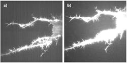
Backside illumination approaches the problem differently. By flipping the pixel design upside down, the wiring and transistors are now below the light-sensitive area of the pixel. This enables a near-perfect 95% QE (see Fig. 1). The challenge with backside illumination is the difficult process of thinning the back of the sensor’s silicon to ensure the light is able to reach the light-sensitive area.
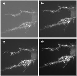
The resulting very high sensitivity not only allows the ability to detect fainter signals, but also provides the flexibility to increase frame rates, or turn down the excitation intensity to reduce cellular photodamage. BSI technology also makes it possible to convert nearly every available photon to useful signal. The camera can maximize the ability to detect weak signals, which enables short exposure times for high frame rates, minimizing cell phototoxicity across a wide range of wavelengths (see Fig. 2).For example, BSI technology is used in Photometrics' Prime 95B Scientific CMOS. This camera offers the extreme sensitivity required for fluorescence microscopy and general bioimaging applications, and a higher a signal-to-noise ratio than the previously dominating EMCCDs. Its high QE means that nearly all incident photons are converted into measurable signal.
Unlike microlens approaches to increase QE, which lose effectiveness as objective magnification is increased, BSI sensors bring light into the pixel photodiode from behind, avoiding structures that reflect or absorb light. When combined with large 11 µm pixels, such imaging devices can deliver three times more signal than other sCMOS cameras at 100 times the magnification.
CMOS, the outperformer at a lower cost
More importantly, scientific CMOS is outperforming EMCCD technology. There is no excess noise that negates the benefit of using a high-QE sensor, and additional limitations from electron-multiplication (EM) gain calibration, stability, expense, and sensor lifetime. With a 16-bit dynamic range, the Prime 95B can accomplish what EMCCD cannot: detect weak and bright signals within the same image with photon-noise limited performance, and all done at a lower cost.
The camera’s 1.6-electron noise floor aids low-light microscopy techniques and, unlike EMCCD cameras, has no multiplication-induced excess noise that destroys measurement precision. A larger field of view with high frame rates allows researchers to track moving objects across the full microscope field of view at better than video rates.
Rachit Mohindra is product manager at Photometrics and QImaging, Surrey, BC, Canada; e-mail: [email protected]; www.photometrics.com and www.qimaging.com.

