Planar metasurface retroreflector could aid communication between remote devices
A team of engineers at the California Institute of Technology (Caltech; Pasadena, CA) is using standard computer-chip fabrication techniques to create compact, flat retroreflectors.1
Retroreflectors' ability to return light to where it came from makes them useful for highlighting objects that need to be seen in dark conditions. They are used, for example, in surveyors' equipment, communications with satellites, and in experiments to measure the distance of the moon from Earth (based on the retroreflector array left on the moon by the Apollo astronauts.
Typically, retroreflectors consist of small glass spheres embedded in the surface of reflective paint, or of arrays of small mirrors shaped like the inner corner of a cube (called "corner-cube reflectors").
The new metasurface technology, developed by a team led by Caltech's Andrei Faraon, assistant professor of applied physics and materials science in the Division of Engineering and Applied Science, uses surfaces covered by a metamaterial consisting of millions of silicon pillars, each only a few hundred nanometers tall. By adjusting the size of the pillars and the spacing between them, Faraon can manipulate how the surface reflects, refracts, or transmits light.
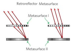
He has already shown that these materials can be tweaked to create flat lenses for focusing light or to create prism-like surfaces that spread the light out into its spectrum. Now, he's discovered that he can build a retroreflector by stacking two layers of the metasurfaces atop one another (see figure above).
In this kind of retroreflector, light first passes through a transparent metasurface and is focused by its pillars onto a single spot on a reflective metamaterial layer. The reflective layer then bounces the light back to the transparent layer, which transmits the light back to its source.
Since Faraon's metamaterials are created using computer-chip manufacturing technologies, it would be possible to easily integrate them into chips used in optoelectronic devices.
"This could have applications in communicating with remote sensors, drones, satellites, etc.," says Faraon.
REFERENCE:
1. Amir Arbabi et al., Nature Photonics (2017); https://dx.doi.org/10.1038/nphoton.2017.96

John Wallace | Senior Technical Editor (1998-2022)
John Wallace was with Laser Focus World for nearly 25 years, retiring in late June 2022. He obtained a bachelor's degree in mechanical engineering and physics at Rutgers University and a master's in optical engineering at the University of Rochester. Before becoming an editor, John worked as an engineer at RCA, Exxon, Eastman Kodak, and GCA Corporation.
