Carbon-nanotube optics poised to provide path to optical quantum cryptography and computing
Researchers at Los Alamos National Laboratory (LANL; Los Alamos, NM) and partners in France and Germany are exploring the enhanced potential of carbon nanotubes as single-photon emitters for quantum information processing, and have analyzed progress in the field.1
"We are particularly interested in advances in nanotube integration into photonic cavities for manipulating and optimizing light-emission properties," says Stephen Doorn, a scientist with the LANL site of the Center for Integrated Nanotechnologies (CINT). "In addition, nanotubes integrated into electroluminescent devices can provide greater control over timing of light emission and they can be feasibly integrated into photonic structures. We are highlighting the development and photophysical probing of carbon-nanotube defect states as routes to room-temperature single-photon emitters at telecom wavelengths."
The team's overview was produced in collaboration with colleagues in Paris (Christophe Voisin) who are advancing the integration of nanotubes into photonic cavities for modifying their emission rates, and at Karlsruhe (Ralph Krupke) where they are integrating nanotube-based electroluminescent devices with photonic waveguide structures. The Los Alamos focus is the analysis of nanotube defects for pushing quantum emission to room temperature and telecom wavelengths, he says.
As the paper notes, "With the advent of high-speed information networks, light has become the main worldwide information carrier. . . . Single-photon sources are a key building block for a variety of technologies, in secure quantum-communications metrology or quantum-computing schemes."
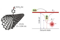
The use of single-walled carbon nanotubes in this area has been a focus for the Los Alamos CINT team, where they developed the ability to chemically modify the nanotube structure to create deliberate defects, localizing excitons and controlling their release. Next steps, Doorn notes, involve integration of the nanotubes into photonic resonators, to provide increased source brightness and to generate indistinguishable photons. "We need to create single photons that are indistinguishable from one another, and that relies on our ability to functionalize tubes that are well-suited for device integration and to minimize environmental interactions with the defect sites," he says.
"In addition to defining the state of the art, we wanted to highlight where the challenges are for future progress and lay out some of what may be the most promising future directions for moving forward in this area. Ultimately, we hope to draw more researchers into this field," Doorn says.
Source: http://www.lanl.gov/discover/news-release-archive/2018/June/0618-carbon-nanotubes.php
REFERENCE:
1. X. He et al., Nature Materials (2018); doi: 10.1038/s41563-018-0109-2.

John Wallace | Senior Technical Editor (1998-2022)
John Wallace was with Laser Focus World for nearly 25 years, retiring in late June 2022. He obtained a bachelor's degree in mechanical engineering and physics at Rutgers University and a master's in optical engineering at the University of Rochester. Before becoming an editor, John worked as an engineer at RCA, Exxon, Eastman Kodak, and GCA Corporation.
