Solution process easily fabricates ceramic films for organic solar cells
Organic photovoltaic (OPV) cells have several advantages over silicon-based solar cells: they are lightweight and flexible and their production cost is low. For these reasons, they could become the next generation of PV cells.
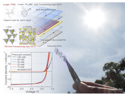
In addition to organic semiconductors that absorb light, OPV cells require materials for buffer layers (buffer layers, or OPV inter-layers, efficiently separate electrons and holes produced from light energy and transport electrons and holes to each electrode). One fabrication approach that has caught the attention fo researchers is a spin-coating technique to create zinc-related oxide (ZnOx, ZnOHx) ultrathin films (ceramic films) using a solution.
OPV cells using ZnO thin films as buffer layers are actively being studied. In conventional production processes of ZnO thin films, a sintering process using high-temperature heating or alternative types of energy irradiation has been necessary.
Now, a joint group of researchers from Osaka University and Kanazawa University has developed a technique for coating zinc related oxide simply by depositing the films in a solution process using a metal organic decomposition (MOD) method at ambient temperature and pressure (no heating whatsoever). They also demonstrated that thin films produced by this technique were useful as buffer layers for OPV cells and that the films achieved a power-conversion efficiency (PCE) equivalent to that of ZnO thin films produced by conventional methods involving sintering.1
The thickness of this ultrathin film can be controlled within the range of 5 to 100 nm. OPV cells were created using this film-making technique, achieving the highest PCE using a film about 20 nm thick. The technique should drastically reduce production process complexity and cost.
Source: http://resou.osaka-u.ac.jp/en/research/2018/20180721_1
REFERENCE:
1. Makoto Karakawa et al., Scientific Reports (2018); https://doi.org/10.1038/s41598-018-27953-6

John Wallace | Senior Technical Editor (1998-2022)
John Wallace was with Laser Focus World for nearly 25 years, retiring in late June 2022. He obtained a bachelor's degree in mechanical engineering and physics at Rutgers University and a master's in optical engineering at the University of Rochester. Before becoming an editor, John worked as an engineer at RCA, Exxon, Eastman Kodak, and GCA Corporation.
