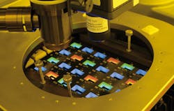
Electron-beam patterning causes OLED surface to emit red, green, or blue
OLED microdisplays are increasingly being used in consumer-ready wearables and data glasses. To meet the requirements for higher efficiency, higher contrast, and higher resolutions in these applications, scientists at Fraunhofer Institute for Organic Electronics, Electron Beam and Plasma Technology (Fraunhofer FEP; Dresden, Germany) have developed a new micropatterning approach for OLEDs on silicon substrates.
The new technique could eliminate the use of color filters and shadow masks in the future and allow full-color displays to be developed by means of a new process. An increase in efficiency and considerably broader color gamut have already been demonstrated in the first experiments. The results will be presented at the Fraunhofer FEP booth no. 50 and during the poster session at IMID 2018 (Busan, South Korea; August 29-31, 2018).
OLED microdisplays are well-suited for use in data glasses for current and future virtual-reality (VR) and augmented-reality (AR) applications. Thanks to the shallow overall depth that results from the self-luminous properties of OLEDs and their high contrast ratios, manufacturers are increasingly turning to OLED microdisplays for AR/VR glasses. Fraunhofer FEP has been immersed in the advanced development of this technology for several years; nevertheless, there are still technological challenges that need to be mastered in order to exploit the full potential of OLED technology for use in consumer-ready data glasses and other AR/VR applications. Very high brightness and efficiency, good yields for large chip areas, curved surfaces, integrated eye tracking, and transparent substrates are some of the tasks still on the researchers' agenda.
Currently, full-color OLED displays can only be realized by using color filters or shadow masks, which limit OLED efficiency and resolution. Researchers are working on new approaches to fabricate microdisplays that have high resolution while at the same time offering high efficiency and long operating lifetime. The patterning of the organic layers of OLEDs is one of the greatest challenges, since conventional methods such as photolithography cannot be used with organic semiconductor materials. The use of electron-beam technology for microstructuring was successfully demonstrated at the Fraunhofer FEP two years ago. Using its patented process, FEP was able to modify the emission of an OLED through the existing encapsulation layer to create any feature imaginable and even produce high-resolution grayscale images.
Further development of the electron-beam process has now achieved full-color OLEDs without using color filters or shadow masks. To create red, green, and blue pixels, an organic layer of the OLED itself is ablated by a thermal electron-beam process. This patterning causes a change to the thickness of the layer stack, which makes the emission of different colors possible. This is the first major step towards the development of full-color displays without the use of restrictive color filters in the process.
The main goal in the coming years is to use this new method in jointly developing fabrication of OLED microdisplays with partners and establish it in the industry through licensing. To do this, the features will be further miniaturized and the process optimized by working together with interested partners from industry. The next step planned is to integrate the micropatterning into existing processes in order to gain further know-how jointly with industrial partners. This should enable future transfer of the test results into an existing process line to be worked out in order to facilitate establishing the technology at the industrial level at a later date.
In parallel, the scientists are also planning an enhanced simulation of OLEDs. The OLED color spectrum will be broadened by suitably modifying the materials and layer thicknesses. In this way, the prospective incorporation the displays in data glasses for special applications such as in industrial manufacturing and medicine should be opened up with the new process.
The development of the new technology is the result of a project funded by the Fraunhofer-Gesellschaft. Now the scientists are ready for specific advanced development of the technology through partnerships and joint projects with display, plant, material and system manufacturers. The results with first colored OLEDs will also be presented at the Fraunhofer FEP booth no. 50 and in poster session III during the International Meeting on Information Display - IMID 2018 in Busan, South Korea, August 29-31, 2018.
Source: https://www.fep.fraunhofer.de/en/press_media/13_2018.html?utm_campaign=pm1813en

John Wallace | Senior Technical Editor (1998-2022)
John Wallace was with Laser Focus World for nearly 25 years, retiring in late June 2022. He obtained a bachelor's degree in mechanical engineering and physics at Rutgers University and a master's in optical engineering at the University of Rochester. Before becoming an editor, John worked as an engineer at RCA, Exxon, Eastman Kodak, and GCA Corporation.
