Wireless self-charging system uses near-IR light and quantum dots
Wireless charging is becoming more commonplace, especially for wearable electronic devices. Researchers from Korea Advanced Institute of Science and Technology (KAIST; Daejeon, Korea) have now developed a wireless self-charging platform for low-power wearable electronics in which near-infrared (near-IR) light is converted to electrical energy using colloidal quantum-dots (CQDs). The novel technology can be applied to flexible, wearable charging systems without needing any attachments.
CQDs are promising materials for manufacturing semiconductors; in particular, lead sulfide (PbS)-based CQDs have optical tunability from the visible to infrared wavelength region. As a result, they can be used in various devices such as lighting, photovoltaics (PVs), and photodetectors. Research on CQD-based optoelectronic devices has increased their power conversion efficiency (PCE) to 12%; however, applicable fields have not yet been found for them.
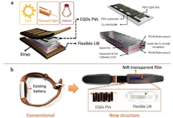
A joint team led by Professor Jung-Yong Lee from the Graduate School of Energy, Environment, Water and Sustainability and Jang Wok Choi from Seoul National University decided to apply CQD PVs with high quantum efficiency in the near-IR band to self-charging systems on wearable devices. The system was composed of a PbS CQD-based PV module, a flexible interdigitated lithium-ion battery, and various types of near-IR-transparent films.
The team removed the existing battery from an already commercialized wearable healthcare bracelet and replaced it with the self-charging system. They confirmed that the system worked and had high photostability and efficiency.
"I believe that this will be a novel platform for energy conversion and that its application can be further extended to various fields, including mobiles, IoT (Internet of Things), and drones," says Lee.

John Wallace | Senior Technical Editor (1998-2022)
John Wallace was with Laser Focus World for nearly 25 years, retiring in late June 2022. He obtained a bachelor's degree in mechanical engineering and physics at Rutgers University and a master's in optical engineering at the University of Rochester. Before becoming an editor, John worked as an engineer at RCA, Exxon, Eastman Kodak, and GCA Corporation.
