Automation streamlines subassembly production
Automation streamlines subassembly production
Small-volume clean areas, standardized component-handling trays, and automated assembly, test, and measurement procedures improve manufacture of optical subassemblies.
James F. Dormer
According to projections, the North American market for optoelectronic components is expected to reach $5.9 billion by 2004 (see Laser Focus World, Feb. 1996, p. 47). Production, meanwhile, is expected to lag behind at $2.7 billion per year. Although sophisticated processes are used to produce the diode lasers and other elements used in such components, devices are typically assembled and tested by hand in a labor-intensive process that slows production and potentially reduces yield.
In 1995, Lucent Technologies engineers representing manufacturing, development, and research were asked to revamp the design and manufacture of optical subassemblies (OSAs) used as a fundamental building block for a variety of high-performance cooled laser package families. The team focused on redesigning the OSA for manufacturability, redesigning the manufacturing facility itself, and redefining the facility infrastructure. The result of this effort is Laser 2000, the Lucent Technologies Microelectronics Group automated manufacturing facility in Breinigsville, PA.
Laser 2000 is a state-of-the-art packaging and testing platform for the manufacture of analog, digital, and electroabsorptive-modulated OSAs. Lucent has incorporated process automation for efficiency and consistency; small-scale, clean process environments to eliminate costly cleanrooms; and a redesigned chip to facilitate automation. The approach has reduced cost and delivery intervals while improving product performance. The new facility will also allow future integration of silicon optical-bench and optical-waveguide technologies for next-generation products.
Module redesign
Design of this new family of products began with the goals of minimizing cost to allow entry into the economical uncooled laser market, standardizing product design with the emphasis on ease of manufacture, and meeting quality expectations through process characterization and testing. Traditional redesign methods that focus on reducing the cost of piece parts could not keep pace with customer expectations for continuous price reductions. The only effective design approach required the elimination of piece parts and the simplification of the manufacturing process.
Conventional laser modules consist of a source and mount, optical components to condition the source output, a feedback loop with detector, and a substrate. To minimize part content for the OSA, engineers stripped the design down to a diode laser, a photodiode for monitoring laser operation, an optical element, and a substrate. The result was a planar design that eliminated the need for a laser submount and a photodiode submount. This type of device can be manufactured with top-down, or layered, assembly processes that are compatible with pick-and-place techniques; it is also designed to be compatible with the uncooled laser in a miniature dual inline package manufactured by FiNet Technologies [a Lucent Technologies and Furukawa Electric partnership].
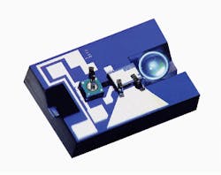
Silicon was chosen for the substrate to take advantage of the crystallographic nature of the material as well as existing support technology. An etched cavity in a silicon optical bench holds a spherical lens to collimate laser output. The diode laser is bonded to the silicon with a high-temperature solder--no epoxy is used in the OSA assembly process. Special alignment features on the laser and the silicon optical bench expedite assembly and minimize positioning error. The photodiode is bonded in the plane of the silicon optical bench (see Fig. 1).
The resultant optical subassembly can be optically and electrically characterized to predict final package performance. More than seven patents have been issued or applied for in association with the design and manufacture of the OSA. Throughout the design phase and subsequent manufacture, testing and process characterization were used to establish specifications, capabilities, and process models that resulted in significant improvements in yield and component quality.
Standardization in manufacturing
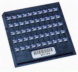
Material handling of the OSA was an important consideration in the development of the new facility. An entire OSA is only 2.5 ¥ 3.5 mm, and, during assembly and testing, the modules are vulnerable to electrostatic discharge (ESD) and to particulate contamination. To protect the devices while simplifying handling, engineers designed a 2 ¥ 2-in. ESD-safe waffle pack to hold the OSAs (see Fig. 2). Automated assembly and test facilities for Laser 2000 were designed to use this pack as a handling vehicle, permitting complete hands-off processing of OSAs without loss or damage.
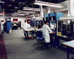
Many of the assembly steps for OSAs must be performed in a low contamination environment, traditionally a cleanroom. This requirement contributes to the cost of the final component, as the expense of maintaining extensive cleanroom facilities is high compared to that for noncleanroom work areas. Lucent designers took an alternative approach, scaling down a conventional cleanroom to the minimum volume necessary to hold production equipment (see photo on p. S7). All assembly and test operations requiring a low contamination environment are performed in these modules, but the factory floor outside is ordinary workspace.
The use of the small-volume clean areas replaces the need for multiple air handlers and return air chases required in traditional laminar-flow cleanrooms. An air-handling unit supplies the purified air required for the workstation clean environments. High-efficiency purified-air filters further filter the air at the point of use. The waffle-pack handling units are placed in the clean area by production staff, and the robotic arm removes parts from the pack as appropriate, or performs testing in situ.
Eliminating the cleanroom requirement allowed facility designers to add flexibility in the choice of construction materials as well as to improve working conditions. For example, the static dissipative carpet now used throughout the facility is easier to maintain than a tile floor and provides a more comfortable working environment. Personnel no longer need to wear traditional cleanroom attire--smocks for ESD protection are sufficient. Engineering and management offices typically banned from cleanrooms due to the inability to control paper and other contaminants, are now located directly on the facility floor, providing enhanced communication among design and production personnel.
Automation in action
The automated manufacturing process begins at the assembly station. Trays of components for the OSAs fabricated at other Lucent facilities are placed in the clean environment of station #1. A gantry robot (right foreground of photo on p. S7) mounts the laser, photodiode, and lens in the silicon optical bench and bonds the components in place with micron-level precision. It inserts the completed module into a slot in the waffle pack. The OSAs remain in this pack though all subsequent steps.
In station #2, the production equipment bonds gold ribbons to the laser and the photodiode. Modules undergo burn-in at station #3 before moving into the testing flow, which takes place at dedicated stations. Each OSA is tested for continuous-wave power, output wavelength, and performance (bit-error rate, bandwidth, and so on). Test points on the silicon optical bench are standardized across all product codes, so test equipment is compatible with the full range of product families, increasing the effectiveness of capital equipment use.
An Intranet links all test equipment, and OSAs can be characterized for a variety of custom applications without removal from the handling vehicle. Subsequent to characterization, a code-sorting facility uses the centrally stored test data and sorts devices based on customer-specific performance criteria. This is especially useful for the dense wavelength-division multiplexing market--OSAs can be sorted by channel without manual handling.
After completion of testing, the OSAs move to the final assembly station for packaging. A gantry robot based on the same equipment platform used for the OSA assembly step bonds the OSA and other package-specific components to the inside of the package body. This automated assembly step replaces hand and mechanized operations used in previous generations of products and integrates the assembly of components within the package body in one step.
It is rare to have an opportunity to completely re-engineer the way in which a product is manufactured. Many of the same team that developed the product continue to support the manufacturing, thus eliminating the typical transfer of product and process design from the development community to the manufacturing community. The automated assembly and test facility results in substantially improved production yields, product uniformity, and throughput. o
Optoelectronic-component manufacturing facility cuts cost and increases yield by standardizing component design and handling trays, automating assembly, test, and measurement, and replacing cleanrooms with small-volume clean areas around production equipment (right).
FIGURE 1. Planar design of revamped optical subassembly is compatible with automated assembly techniques, eliminating the need for separate laser (center) and photodiode (left) mounts and incorporating alignment features on the laser and the silicon substrate to facilitate device assembly. These features include a mounting cavity for the focusing optic (right).
FIGURE 2. Waffle pack holds 50 optical subassemblies during the automated assembly and test process.


