Microscopy: Multi-frequency NSOM maps optical forces without a photodetector
Near-field scanning optical microscopy (NSOM) uses a sharp probe tip or a small aperture to scatter the electromagnetic field near the surface of a sample to gather high-spatial-resolution information present in the surrounding evanescent field. The subwavelength field information is then converted to a propagating far-field and measured with a photodetector to image the sample.
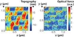
In a new technique called multifrequency NSOM, researchers at the College of Optics and Photonics (CREOL) at the University of Central Florida (UCF; Orlando, FL) and CNRS Institute Langevin (Paris, France) apply both an electrical signal and an optical signal to the tuning-fork architecture to map both surface topography and the spatial distribution of optically induced forces acting on the probe.1 Because the method does not require a photodetector for radiation-distribution mapping, broadband detection of light is possible using a single probe.
Optically induced force measurement
In the experimental setup, an oscillating quartz tuning fork with a sharp probe tip (a conventional gold-coated, pulled-fiber 100-nm-diameter aperture) affixed to one arm is piezoelectrically driven just above the sample surface and the probe position is maintained through a feedback mechanism for the first resonance signal to enable surface topography mapping as in standard atomic force microscopy (AFM). When a second oscillation is applied to the probe tip on one arm of the tuning fork, an additional higher-order resonance can be monitored that yields information on the forces acting upon the tip.
The probe is situated above the sample surface and is illuminated by 635 nm laser light coupled out of a single-mode fiber and maintained at an intensity of 0.36 mW/μm2. While the electrical signal enables topography mapping, the amplitude and phase of the optically induced resonance signal depend directly on the optical force acting on the tip.
Using standard coupled equations of motion for the damped, driven NSOM harmonic oscillator that include both the electrical and optical frequency parameters, the amplitude and phase of the optical signal can be obtained. From variations in these two values, the magnitude of the optical force acting on the probe and its gradient can be extracted, yielding information on optical forces occurring spatially within the sample under test.
In an experiment, the force distribution was measured across a gold nanosphere lithography sample consisting of 0.453-μm-diameter gold spheres placed against a glass substrate and separated with 260 nm center-to-center spacing. Using both a tuning fork and a cantilevered-probe NSOM, near-field optical forces were measured with better than wavelength/50 resolution.
In the context of NSOM practice, CREOL professor of optics Aristide Dogariu says, “This multifrequency approach permits measuring—simultaneously—multiple aspects of the near field in the proximity of a sample and it also provides means to decouple the effects of different forces acting on the probe. Most importantly, it allows to separate the possible influence of thermal effects induced by the electromagnetic radiation. Without sacrificing spatial resolution, this technique not only circumvents the need for photon detectors but it also complements traditional approaches for optical characterization of metamaterials, plasmonic nanostructures, and biological structures.”
REFERENCE
1. D. C. Kohlgraf-Owens et al., Nanotechnol., 25, 035203 (2014).

Gail Overton | Senior Editor (2004-2020)
Gail has more than 30 years of engineering, marketing, product management, and editorial experience in the photonics and optical communications industry. Before joining the staff at Laser Focus World in 2004, she held many product management and product marketing roles in the fiber-optics industry, most notably at Hughes (El Segundo, CA), GTE Labs (Waltham, MA), Corning (Corning, NY), Photon Kinetics (Beaverton, OR), and Newport Corporation (Irvine, CA). During her marketing career, Gail published articles in WDM Solutions and Sensors magazine and traveled internationally to conduct product and sales training. Gail received her BS degree in physics, with an emphasis in optics, from San Diego State University in San Diego, CA in May 1986.
