Photonics Products: High-power Laser-Diode Arrays: Diode arrays are compact, high-power light dynamos

High-power laser-diode arrays, which are made of stacks of individual or multistripe laser diodes, or in some cases vertical-cavity surface-emitting lasers (VCSELs), can put out watts to kilowatts of optical power for uses such as laser pumping, industrial heating, illumination, or as the input for fiber-optic direct-diode laser devices for materials processing or for medicine.
Laser diodes typically have much higher electrical-to-optical (wall-plug) efficiencies than other types of lasers; in fact, they are some of the most-efficient light emitters known. The disadvantage of laser-diode arrays is their relatively low beam quality—there are no single-mode kilowatts-level laser-diode sources in our near future. However, there are many applications that do not require a single-mode beam; in addition, laser manufacturers are constantly refining beam-combining techniques to produce ever-brighter high-power laser-diode sources.
From watts to kilowatts
"High-power diode lasers are commonly referred to as being bar-based or single-emitter-based," says Steve Patterson, VP and GM of DILAS (Tucson, AZ). "In point of fact, they exist on a continuum with single emitters on one end and bars—typically a centimeter wide or less, consisting of multiple emitters on a single piece of semiconductor—on the other. The diode lasers are then mounted to any of a variety of heat sinks, the choice depending upon operating conditions and what final package the diode laser bar might go into."
DILAS produces laser bars that range in output power from single-digit values out to hundreds of watts per bar. Their wavelengths range from 635 nm (visible red) to greater than 2300 nm and beyond, with electrical-to-optical efficiency reaching to more than 70% in some cases, notes Patterson.
The mounted bars can then be packaged into arrays that produce up to kilowatts of total output power, whether the output be a free-space laser beam or coupled into an optical fiber. With these sorts of capabilities, says Patterson, "any market from the traditional pumping of solid-state and fiber lasers, to direct-diode applications in medicine such as dermatology or phototherapy, to industrial processing of materials such as the deposition of laminates to emerging markets in cinematography and enhancements in advanced medical-imaging technologies may be addressed."
Patterson notes that there have been many new developments over the past year: for example, enhancements in visible red and blue outputs for applications in cinematography and medical photodynamic therapy; fiber-coupled systems that output on the order of 10 kW in wavelengths ranging from around 800 nm to 1000 nm, typically used for all sorts of materials processing, including welding; and a unit developed to enhance magnetic-resonance imaging (MRI).
"All aspects of diode-laser technology were challenged here," says Patterson. The challenges included development of the basic epitaxy design of the diode laser, advances in the volume Bragg gratings that narrow the spectral line of the diode laser to a range that is useful for the particular application, custom package design that permits tunability of the spectral line emitted from the module, and the custom optics that form the beam to a precise output form also demanded by the application.
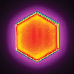
Patterson provides background on the MRI module (see Fig. 1), explaining that it permits the hyperpolarization of a particular isotope of xenon using a process called spin-exchange optical pumping; the spectrally narrowed and precise wavelength of circularly polarized laser light from the module excites rubidium electrons inside a gas cell. The use of hyperpolarized gas in MRI allows observation of otherwise inaccessible bodily processes, such as pulmonary function and blood profusion in the brain. The module itself emits 200 W of circularly polarized light at a 794.7 nm wavelength and a linewidth of <0.3 nm; the optically isolated beam is tolerant to 100% backreflection.
Direct diode
While laser-diode bars are used widely as laser pump sources, by using the right optical techniques, light from the same sorts of diodes can be directly coupled into optical fibers to produce a high-power "direct-diode" laser, notes Tracey Ryba, product manager for lasers at the TRUMPF Laser Technology Center (Plymouth, MI). For example, the same 940 nm diode-bar platform used by TRUMPF as pumps for its disk lasers is the source for the company's kilowatts-level direct-diode systems.
Optical techniques for combining laser-diode outputs to boost power while maintaining brightness include spatial and spectral beam combining. However, the details, which are derived from careful optical design and which make all the difference in final beam brightness, are usually proprietary.
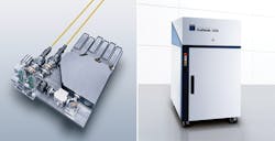
The diode bars in TRUMPF's direct-diode systems are mounted on a passively cooled heat sink, eliminating the need for high-quality deionized (DI) water and eliminating microchannel failure, explains Ryba (see Fig. 2). "The final fiber-coupled direct-diode laser uses wavelength combining of one, two, or three wavelengths depending on power of the laser and varying in wavelengths from 920 nm to 1020 nm," he says. The company's 150 and 300 W direct-diode lasers have a beam-parameter product (BPP) of 8 mm-mrad, while the BPP for the 600 and 900 W lasers is 12 mm-mrad. The high-power 2000–4500 W lasers have a BPP of 30 mm-mrad and the highest-power 3000-6000 W model has a BPP of 50 mm-mrad."Lasers ranging from 150 to 300 W typically are used for plastic welding, soldering, and other low-power welding applications," says Ryba. "Between 600 and 900 W, the ideal applications are thin-metal welding and low-volume cutting. The 30 mm-mrad models are used for deep-penetration and heat-conduction welding, heat treating, and laser metal deposition, while the 50 mm-mrad applications typically are brazing, heat treating, and laser metal deposition."
Wavelengths in the "9xx" nm wavelength range are slightly shorter than those of traditional 1 μm lasers such as disk, fiber, and Nd:YAG. These shorter wavelengths allow better absorption in highly reflective materials such as copper, brass, and aluminum, says Ryba. Additionally, the lower-beam-quality versions are ideal for brazing and surface treatments due to the large divergence and the more distinct flat-top mode profile, especially when compared to high-beam-quality disk and fiber lasers where a relatively complex beam delivery and large focal lengths are needed to achieve the same desired effects at the workpiece.
Replacing traditional processes
The attributes of high-power laser diodes can lead to transformations in certain areas of materials processing. "Major 'direct-diode' applications for these products are transforming the surface properties of large metal parts through heat treating—historically called case hardening—and cladding," explains Frank Gaebler, director of marketing at Coherent (Santa Clara, CA).
Coherent manufactures laser diodes and laser-diode arrays over a broad range of output powers in configurations from single emitters through linear bars (fiber-coupled and free-space) up to 2D arrays of bars. The company's most powerful system produces 10 kW of output power at 975 nm; internally, it consists of five bars, each derated to 2 kW to ensure tens of thousands of hours of maintenance-free operation at or above specified power, says Gaebler.
The free-space output of the laser system can be configured to deliver a variety of interchangeable beam shapes (with widths from 1 to 12 mm and lengths from 6 to 36 mm) to enable rapid processing of large areas with a high degree of control over process parameters.
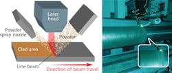
The product is targeted at large-area cladding applications to create a metallurgically bonded layer on the surface of a metal, usually some type of steel (see Fig. 3). "This is typically done in order to transform the surface properties—for improved wear characteristics or high corrosion resistance—without modifying the desirable bulk properties (such as tensile strength and rigidity) of the part," says Gaebler. "Cladding is also often used to refurbish worn parts."Traditionally, large parts were mainly clad by thermal spray (for example, high-velocity oxygen-fuel spraying, or HVOF) or plasma-transfer arc (PTA) or, less commonly, electroplating, as Gaebler explains. Thermal spraying is a fast and relatively cheap process where metal powder is melted and sprayed on to the substrate, where it solidifies. The problems are that the coating is not metallurgically bonded to the surface, which limits its long-term wear resistance, and, in addition, the final coating has varying degrees of porosity, which can compromise its corrosion resistance.
In contrast, the laser-diode approach not only melts the powder, but also melts a very thin outer layer of the substrate, producing a fully bonded layer with very low porosity.
Giantree Laser Technology (Shanghai, China), one of the leaders in laser cladding applications in China, has extensive firsthand experience with laser cladding, thermal spray coating, machining/grinding, and materials/alloys know-how, says Gaebler.
Giantree now has two in-house laser-cladding systems based on high-power direct-diode lasers, including a 10 kW unit from Coherent. Giantree services clients in several heavy industries, such as petrochemicals and coal mining. Typical high-value components that require cladding are the hydraulic roof supporters used to prevent collapse of tunnels and galleries (see Fig. 3). Giantree coats both the cylinders and pistons of roof supporters with materials such as stainless steel for better corrosion resistance.
Until recently, electroplating had been Giantree's first-choice method for coating these supporters. According to Kenneth Liao, manager of Giantree, "Simply stated, laser cladding delivers better corrosion resistance, and thus longer lifetime for these supporters because it produces a full-density coating, which electroplating typically doesn't."
VCSEL arrays for imaging and gesture recognition
High-power laser-diode arrays don't have to be made up of edge-emitting diodes. For example, Princeton Optronics (Mercerville, NJ) makes arrays of vertical-cavity surface-emitting lasers (VCSELs) for illumination and other purposes.
"One major high-volume application of laser diodes is for 3D imaging and gesture recognition with computers, tablets, and cell phones," says Chuni Ghosh, the company's CEO. "Projects like Google Project Tango and Intel RealSense are platform technologies that are being adapted by manufacturers for production in the near future. VCSEL arrays are particularly suited for such applications."
Depth sensing is done by structured light, time of flight, and stereoscopic approaches, explains Ghosh. "VCSELs have advantages compared to other technologies in all three approaches. The advantages come from being able to surface-mount the devices (versus TO-can packaging of edge emitters), which makes the height very small." A height of 3 mm or less is needed for the complete illuminator with the projection lens, he adds.
The VCSELs produced by Princeton Optronics have a wall-plug efficiency of >40% at a temperature of 60°C and a reliability (mean time to failure, or MTTF) of more than 100 years for operation at 70°C; these figures are achieved "with some proprietary process innovations," says Ghosh.
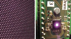
In structured-light applications, a pattern of spots is projected onto the object of interest (see Fig. 4); using a camera, the depth is estimated from the distribution and shape of the spots. For time-of-flight measurements, very fast rise and fall times are needed, explains Ghosh. VCSEL arrays give very fast rise and fall times, typically <300 ps, and rise and fall times of <100 ps can be obtained with low-inductance submounts.VCSEL arrays also have a narrow emission wavelength (<1 nm) and low variation of the wavelength peak with respect to temperature (0.07 nm/°C), which helps to reject the background illumination when the camera chip is attached with a narrowband filter.
Princeton Optronics' technology has been developed with funding from the U.S. Defense Advanced Research Projects Agency (DARPA) and other agencies, says Ghosh. "We have developed VCSEL chips with power levels as high as a kilowatt from a 5 × 5 mm array with a greater than 55% wall-plug efficiency," he notes. "This technology is being used to make many different types of products for 3D imaging applications."
One such product is an 8 W VCSEL array used for time-of-flight as well as structured-light applications. The laser chip is 1.5 × 1.5 mm in size, has a large number of VCSEL devices, and is mounted on a surface-mountable ceramic substrate. The device is finding application in computers, tablets, and mobile phones.

John Wallace | Senior Technical Editor (1998-2022)
John Wallace was with Laser Focus World for nearly 25 years, retiring in late June 2022. He obtained a bachelor's degree in mechanical engineering and physics at Rutgers University and a master's in optical engineering at the University of Rochester. Before becoming an editor, John worked as an engineer at RCA, Exxon, Eastman Kodak, and GCA Corporation.


