Random Lasers: Diamond supplies holes for electrically pumped ZnO laser

A random laser contains a gain material (such as a polycrystalline material and/or a material with a rough surface) in which scattered light takes random paths, forming many small laser cavities (which can be in the form of loops) and resulting in diffuse laser light. Random lasers have uses in sensing and biomedical imaging. The most well-known random lasers use zinc oxide (ZnO) as the gain medium and emit near-ultraviolet light.
However, the typical random laser is optically pumped, which makes the whole experimental setup far bulkier and more complex than it could be. Some working ZnO electrically pumped random lasers have been made by p-type (hole) doping of ZnO, which is intrinsically an n-type (electron-providing) semiconductor, but the result is not very efficient.
Now, a group of Chinese researchers at the Chinese Academy of Sciences (Changchun and Beijing), Zhengzhou University (Zhengzhou), Jilin University (Changchun), Fudan University (Shanghai), Changchun University of Science and Technology (Changchun), and the Inner Mongolia University for Nationalities (Tongliao) has taken an excellent source of holes—p-doped diamond—and mated it to ZnO core-shell nanowires with magnesium (Mg)-doped shells to create an electrically pumped random laser that has a good supply of both electrons (ZnO) and holes (diamond). When the electrons and holes combine, laser light is produced.
Boron-doped diamond
To create holes, the diamond was doped with boron to 0.5 wt. %; the resulting material took about 24 hours to grow to its 3 mm size using a temperature-gradient synthesis method. The diamond was then cut and polished to a thickness of 1 mm. The ZnO nanowires were grown on a separate sapphire substrate and then coated with the Mg-doped layer to form a heterostructure.
The nanowires were crystallized in a wurtzite structure with a c-axis preferred orientation; the 3.6-μm-long wires were oriented parallel with each other and perpendicular to the substrate. The photoluminescence spectrum of the nanowires showed the expected sharp peak at 378 nm because of the near-band edge emission of the ZnO. A so-called "deep-level" emission at around 500 nm, which is an indication of poor-quality fabrication, was almost entirely absent.
As a preliminary test, ZnO nanowires were optically pumped at varying intensities, producing sharp peaks at 383.7 and 387.2 nm, with the light emitting in a 60° cone aligned with the nanowires. Such a light cone is characteristic of random lasers.
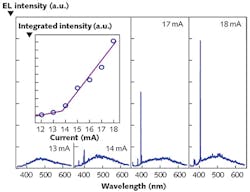
Next, the core-shell nanowire heterostructures were placed in pressure contact with the boron-doped diamond using a clip to hold it all together. The assembly was subjected to a voltage of about 6 V via an indium pad on the ZnO potion and a gold pad on the diamond. Below the laser threshold at an injection current of 13 mA, a broad spectrum with a full-width half-maximum (FWHM) of 138 nm was the result; at an injection current of 14 mA, two sharp peaks near 400 nm appear, each with a FWHM of 0.9 nm. The two peaks are red-shifted from the earlier-measured photoluminescence peaks, which the researchers attribute to heating of the device by current injection.
REFERENCE
1. Y.-J. Lu et al., Optica (2015); http://dx.doi.org/10.1364/optica.2.000558.
About the Author
John Wallace
Senior Technical Editor (1998-2022)
John Wallace was with Laser Focus World for nearly 25 years, retiring in late June 2022. He obtained a bachelor's degree in mechanical engineering and physics at Rutgers University and a master's in optical engineering at the University of Rochester. Before becoming an editor, John worked as an engineer at RCA, Exxon, Eastman Kodak, and GCA Corporation.
