Reconfigurable microfluidic metasurfaces create tunable color displays
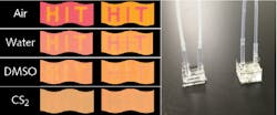
Despite rapid progress in creating color images from nano- or microstructured materials—a process called structural color—the optical characteristics of most nanostructures are static once they are fabricated, severely restricting their use in stereoscopic imaging, animation, point-of-care, and anticounterfeiting applications. But by integrating microfluidic channels with titanium dioxide (TiO2) metasurfaces, researchers at the Harbin Institute of Technology (Shenzhen, China) are now able to create displays with distinct and high-resolution tunable colors and rapid transition time.
The metasurface is composed of an array of TiO2 nanoblocks that are embedded in a polymeric microfluidic channel. By injecting solutions with different refractive indices into the channel, the narrowband reflection peak and the corresponding distinct colors of a TiO2 metasurface can be precisely controlled. The transition time between color changes is as small as 16 ms—orders of magnitude faster than competing techniques and suitable for real-time display applications. Varying the lattice size of the TiO2 metasurfaces enables display of real-time tunable colors that span the entire visible range, and the injection and ejection of solvent in the channels allows erasure and restoration of information encoded in the TiO2 metasurfaces. Reference: S. Sun et al., ACS Nano online (Feb. 2018); doi:10.1021/acsnano.7b07121.

Gail Overton | Senior Editor (2004-2020)
Gail has more than 30 years of engineering, marketing, product management, and editorial experience in the photonics and optical communications industry. Before joining the staff at Laser Focus World in 2004, she held many product management and product marketing roles in the fiber-optics industry, most notably at Hughes (El Segundo, CA), GTE Labs (Waltham, MA), Corning (Corning, NY), Photon Kinetics (Beaverton, OR), and Newport Corporation (Irvine, CA). During her marketing career, Gail published articles in WDM Solutions and Sensors magazine and traveled internationally to conduct product and sales training. Gail received her BS degree in physics, with an emphasis in optics, from San Diego State University in San Diego, CA in May 1986.
