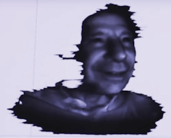
Facial Recognition: 3D TOF camera technology improves facial recognition accuracy and security
Just like light detection and ranging (lidar) can be used to distinguish between the side of a truck in close proximity to a moving vehicle as opposed to mistaking its blue color for a distant clear sky, for example, time-of-flight (TOF) imaging cameras can ensure that facial recognition systems distinguish between an actual three-dimensional (3D) face and a 2D video or photo of a face. Using its epc660 TOF imaging chip and careful calibration, Espros Photonics (Sargans, Switzerland) is building 3D facial scanning systems that offer high spatial accuracy and depth security.1
2D vs. 3D imagers
Traditionally, facial recognition data is acquired with 2D imagers. If additional 3D data is needed, the person to be identified must turn his/her head so that imaging algorithms can extract 3D data as an additional observing and identifying parameter. That is, these algorithms can determine whether the image is a mask or 2D photo as opposed to a living face by taking two 2D images from (slightly) different perspectives and applying a correlation algorithm that acquires depth information that can be used to compute a 3D image (see figure).
The problem starts when this identifier camera looks to screens that display videos with exactly this 3D data information. In such a case, the locking system cannot distinguish between a fake and reality. In general, by using two 2D cameras, both cameras can be fed by two 2D images, with the identification algorithm then calculating the 3D image and comparing this image with the stored key data. If the image matches, the device is unlocked.
Fortunately, TOF imagers avoid these security issues altogether by recording pixel-by-pixel distance information of the object being scanned. A nose extends a greater distance from the face than the eyes, for example. To gather this data, the TOF camera can determine if the 3D model is a static mask or a living person based on the time-domain data.
TOF camera calibration
Using the epc660 TOF chip, a lens, and a vertical-cavity surface-emitting laser (VCSEL) or LED-based illumination system, Espros has developed the DME 660 3D TOF distance measurement camera with a QVGA resolution of 320 × 240 pixels, 94° × 69° field of view, and up to 10 m operating range. With a 36 MHz modulation frequency and open-source hardware and software, more than 156 TOF images can be gathered per second with a distance resolution of 0.13 mm at a quantum efficiency of more than 50% at 940 nm and 100% fill factor without microlenses.
To obtain the best image quality, 3D TOF camera calibration and compensation is essential.2 Numerous calibration parameters are stored in the camera for each individual pixel, including dark-signal offset and gain and color correction. Because the object distances are sensitive to signal delays on the order of 10 to 100 ps (1.5 mm to 1.5 cm distance changes, respectively) due to wiring-length differences between different parts of the pixel array, calibration is needed in that distance errors are also a function of temperature—that is, electron mobility in silicon is highly temperature-dependent.
Espros uses on-chip delay locked loop (DLL) functionality integrated on its TOF image sensors for camera calibration. Here, the DLL capability introduces a “virtual” distance offset by adding a time delay into the modulation or demodulation path that simulates a distance change of the target. Instead of using a moving object on a linear stage, a 30-cm-long passive calibration box that shields the camera from ambient light and provides an optical reference plane in front of the sensor with flat-field illumination is all that is required.
“Through a step-by-step delay of the illumination signal through the DLL, a phase shift is added between the modulation and demodulation of the light signal,” says Beat De Coi, CEO of Espros. “This modulation path delay is essentially equivalent to distance changes for object points, allowing pixel-by-pixel calibration across the sensor.”
REFERENCES
1. See https://goo.gl/VEnFHp.
2. See https://goo.gl/JuehKu.

Gail Overton | Senior Editor (2004-2020)
Gail has more than 30 years of engineering, marketing, product management, and editorial experience in the photonics and optical communications industry. Before joining the staff at Laser Focus World in 2004, she held many product management and product marketing roles in the fiber-optics industry, most notably at Hughes (El Segundo, CA), GTE Labs (Waltham, MA), Corning (Corning, NY), Photon Kinetics (Beaverton, OR), and Newport Corporation (Irvine, CA). During her marketing career, Gail published articles in WDM Solutions and Sensors magazine and traveled internationally to conduct product and sales training. Gail received her BS degree in physics, with an emphasis in optics, from San Diego State University in San Diego, CA in May 1986.
