Manufacturing Photonics: Challenges for photonics manufacturing in the new data center era
YI QIAN
The data generated by the exponential growth rate of Internet traffic is enormous and data centers are crucial to support the resulting data communications, storage, and processing needs through cloud computing. Photonic devices play vital roles in these data centers, and this has posed significant challenges to photonics high-volume manufacturing (HVM).
A recent Cisco study indicates that both global IP and global data center traffic are growing at a compound annual growth rate of around 25%. The proliferation of emerging applications, such as the Internet of Things (IoT), video streaming, 3D sensing, smart cars, and virtual reality (VR) and augmented reality (AR), has created more appetite for bandwidth and thus for new data centers. By 2020, projections show that 50% of data centers will be at the hyperscale level, meaning their architecture will have the ability to scale appropriately as increased demand is added to the system. Approximately 40 hyperscale data centers will be established each year over the next three years.
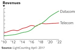
Photonics has been essential for bandwidth growth, historically driven by telecommunications (telecom) and now more by data communications (datacom) fueled by this extraordinary growth in data center business. Figure 1 shows the worldwide sales revenue of optical transceivers for telecom and datacom, respectively. The key inflection point comes around 2017–2019, where the transceiver revenue for datacom surpasses telecom. The study also predicts a significantly higher growth rate for datacom in the future.
Datacom challenges
As data center demand becomes the new growth engine, the photonics industry feels the challenges from servicing new data center business models that are far different from the traditional telecom models. The table summarizes the key differences between the telecom- and data center-centric business models. The most critical factors that impact photonics manufacturing are high volume, low forecast visibility, fast pace of innovation, quick response, and low cost.
Historically, the photonics industry has been strongly influenced by telecom, which has vast field deployments. Because of the difficult operating environment (e.g., -40˚ to 85˚C, RH up to 85%) and thus high cost of system deployment and maintenance, each telecom upgrade cycle is long and carefully planned. The annual forecast visibility from carriers to equipment providers and to component suppliers is fairly good. Sophisticated and expensive photonic components can be accepted during this long cycle. Photonics manufacturers have more time to plan and respond to customer demands, and the unit volume has not been as high as we have seen recently from data center business.
Data center businesses operate the majority of their networks inside of a controlled environment, for example, in temperature- and humidity-controlled buildings (i.e., 0˚–55˚C, RH 40–60%). Most of the capital expenditure (capex) is on land, buildings, and cabling. A large portion of operating expense (opex) goes to energy consumption and environmental control. Photonic components are a relatively small part of capex and opex—however, they are a significant contributor to revenue generation through bandwidth sales to cloud customers.
Comparison of two end-customer business models for the photonics industry
New cloud-based DC model | Traditional telecom-centric model |
|
|
In an office-type of controlled environment, upgrading becomes less expensive. The combination of low replacement cost and low percentage of photonic components in total capex and opex costs makes it possible for data center providers to have an upgrade cycle of three to five years for existing data centers. For each upgrade, they would like to use the most advanced photonics technologies that provide the most possible bandwidth at the time to maximize revenue out of the same building.
It is difficult for a data center provider to predict exactly when a specific data center project will start because a new data center construction project starts with a land survey and acquisition, including approvals from local governments. This significantly reduces forecast visibility to photonic component suppliers. On the other hand, once the project is approved, the data center provider will naturally want to build fast and ramp the revenue stream quickly. After a typical two to three years of construction, the new data center will be ready to go with the most advanced photonics equipment installed that could generate the maximum potential of revenue on day one.
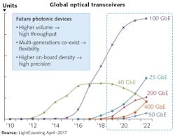
Finally, fast-paced innovations bring the double challenge of high mix and high volume to photonics manufacturing for data center applications. The 40G transceiver upgrade from 10G was the main activity in the past few years (see Fig. 2). Now, 100G is overtaking 40G as the leading technology in new volume deployment. At the same time, 200/400G solutions are at prototyping and low-volume stages. All these different technologies and products will need to coexist for a period of time and will have to pass through the same photonics manufacturing floor.Opportunities and solutions
All of these challenges driven by the new cloud-based data center business model come with opportunities. How can the photonics industry respond to these challenges? The key to addressing these challenges is automation.
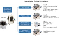
Photonic device suppliers really need to adopt an elastic capacity model that can deliver high-volume, high-quality, low-cost manufacturing with a very fast switch-on-and-off capacity for data centers’ just-in-time model that includes a low forecast visibility (see Fig. 3). Automation can ramp volume fast without worrying about the massive training needed for high-volume manual production. Automation can also lower the dependence on labor to reduce the variable costs, particularly during downtime. In addition, automation minimizes risks for a new product introduction (NPI) because manufacturers can use the same automation platform and process between development and manufacturing phases. Furthermore, high-precision automation enables processes to make advanced products that cannot be made manually.The biggest challenge now facing photonics manufacturing is how to handle the high-volume and high-mix production. The high mix of products typically originates from NPI, or from changeovers between the different products, which makes it difficult to achieve high volume in production because you cannot ramp up production as the configurations keep changing.
Solving this problem requires flexible, high-speed automation. Historically, it has been challenging to put flexibility and high speed together for automatic equipment. A case study will show it is possible to achieve high speed without sacrificing flexibility through innovation in the automation industry.Flexible high-speed die bonding automation platform
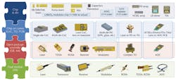
To illustrate our understanding of an automation solution, here is a case study to handle one of the key manufacturing processes—die bonding. Figure 4 is a view of the variety of parts that usually must go through photonics manufacturing. The varieties of these parts result from different types/generations of products to support a wide spectrum of data center communication networks. There are a few major process steps associated with different finished products:
- For Gold Box products such as transceivers with high-power lasers, typically chip-on-carrier/submount (CoC/CoS) bonding is done first and then the CoC/CoS is bonded onto a common baseplate for lens/mirror attachment before putting it into a package. The latest trend is that more chips or dies such as the laser, capacitances, and thermistor need to be attached onto a common carrier by either eutectic or epoxy bonding.
- For PCB level of products such as active optical cable (AOC) and onboard optics (OBO), the dies are attached directly onto a PCB. Multiple dies such as a vertical-cavity surface-emitting laser (VCSEL) array, photodiode (PD) array, laser driver, and transimpedance amplifier (TIA) need to be attached on the PCB. The final lens attachment is done by active alignment historically, but now more and more it is done using passive die attach with the availability of high-speed, high-precision (3 µm) die bonding equipment.
- For TO-can-type products, the laser chip and other dies are attached onto a TO base or the vertical post after 90° flipping. To support upcoming 5G wireless deployment, wavelength-division multiplexing (WDM) lasers and electro-absorption modulated lasers (EMLs) are packaged into low-cost TO-can packaging. With many dies that are required to attach, these WDM/EML-TOs are far more complicated than traditional TO-can packaging that only need to handle 1–2 dies.
- For silicon photonics, more processes are transitioning from CoC form to chip-on-interposer and chip-on-wafer (CoW). Much has still yet to be determined, but the future will rest with more and more wafer level integrations.
Below are three key points to understand how this approach would help respond to the challenges in photonics manufacturing discussed earlier:
- A common platform at both the hardware and software levels can significantly reduce the NPI risks by eliminating the changes of controls or processes already qualified during the development phase. During R&D/NPI phases, the all-in-one type of die bonding equipment can be used to develop multiple types of products. These automatic machines can handle vast types of dies and processes in one piece of equipment. Their speeds are also fast enough to make low-to-medium levels of volume productions for qualifications of design and manufacturing processes. Once the demand arises and high-volume production is needed, the production lines can be organized into specific process groups.
- High-volume, high-mix photonics manufacturing requires flexible high-volume machines that can cover multiple dies, processes, and products through one machine for one or more process groups. The speed and throughput are optimized by introducing an ultrafast eutectic module and deploying multiple levels of parallel processing, such as separating material handling from die bonding steps and integrating tool changing on the fly with zero time wasted.
- The HVM equipment needs to be built for next-generation products for concurrent fast-pace innovations. In this example, the 3 µm placement accuracy is a step up from current mainstream photonics processes using >5 µm placement accuracy. In addition to enabling new products, high precision in die bonding also increases process yields for manufacturing current products by tightening assembly tolerance as early as possible in the process.
In summary, a high-speed automation platform that does not sacrifice flexibility, accuracy, or reliability for 24/7 production is critical to address high-volume, high-mix photonics manufacturing. A common platform between R&D and HVM and the future-proof precision are also critical for fast innovation and reducing NPI risks, and for improving production yields for lower cost in HVM.
Yi Qian is vice president of product management at MRSI Systems, North Billerica, MA; e-mail: [email protected]; www.mrsisystems.com.


