Test & Measurement: Spectrally tunable light sources allow advanced sensor characterization
The need for precision light sources to test image sensors and detectors has existed for decades, but as sensor technologies advance and evolve, requirements for these test sources have intensified. To handle these needs, LED-based tunable light source (TLS) technology has been developed that enables modern sensors to be tested with higher precision, accuracy, and speed than when relying on pre-existing sources.
Here, a few different characterization techniques will be outlined, including color accuracy and Bayer filter spectral mismatch, image-sensor linearity, and frame rate/readout time. The fundamental limits of halogen sources for characterizing silicon charge-coupled device (CCD) and complementary metal-oxide semiconductor (CMOS) sensors will also be outlined.
Traditionally, image sensors need to be characterized for overall performance in some key areas. Determining how the sensor responds to different light stimuli is important to optimize the image captured, whether it be for scientific or consumer applications. In science or machine vision applications, understanding the linearity or timing characteristics can mean the difference between a valid or meaningless result. For consumer applications, color accuracy can be absolutely critical for photography—whether the subject is a human skin tone or vibrant landscape, users will expect the color captured to represent their physical experience.
In all cases, the sensor must be characterized at multiple phases in the production process to ensure a quality end result. Using a stable and precise reference light source is a critical part of those tests, but having tunability in the output intensity or color is also highly desirable. Modern TLS light sources can use LEDs in ways that are more flexible than traditional halogen sources, resulting in higher stability without the drawbacks and problems that were present with early LED reference light sources.
Sensor linearity characterization
One key sensor performance criterion is linearity. Many applications benefit from high linearity, both regarding actual photon-to-electron conversion happening within the chip and the variations in electrical readout relative to exposure time.
To test linearity, a precision light source is swept through a range of different output intensities and the sensor response measured at each power level. The calculated linearity is only as good as the linearity of the light source itself—therefore, the absolute intensity of the light source must be known with high precision and repeatability with low uncertainty. Traditionally, this would be done using a halogen lamp coupled into an integrating sphere, with an iris in between to control intensity. However, a halogen source itself is only stable over short time periods of less than 100 hours, and the iris has mechanical sources of uncertainty as well. In addition, the test time is limited by how quickly the iris can be adjusted and other things like lamp warm-up after collecting a dark background.
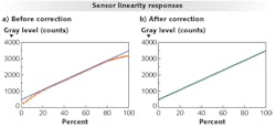
Using an LED-based TLS can overcome these limitations and provide better linearity accuracy than traditional methods. Built-in optical feedback can be used to regulate the LED constant-current drive circuit. Using this closed-loop system with optical feedback adjusting the drive current allows the LED output to be accurately controlled with linearity better than 0.1% of full scale. Feedback also ensures that the absolute output intensity is stable over thousands of hours of operation. Fully solid-state operation means that there are no moving parts to fail and no inaccuracies because of iris mispositioning. The spectrum used for linearity testing can also be tuned, allowing for linearity to be tested with different broadband spectra (such as Illuminant A or D50), or with saturated colors such as red-green-blue (RGB) wavelengths. Figure 1 shows the difference in linearity between a traditional source and the TLS method—note specifically the low-power regions and regions near saturation.
Sensor color accuracy: Bayer filters and spectral mismatch
For some applications, the most important aspect of performance is color accuracy. In those cases, the spectral transmission of the Bayer filter (the color filter array covering the sensor) needs to be carefully determined. There is also much that goes into “demosaicing” algorithms to transform the filtered color channels into what human eyes perceive. Understanding the raw sensor performance is key to proper correction being applied during demosaicing.
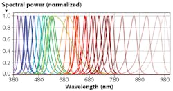
Traditionally, the spectral responsivity or quantum efficiency (QE) of the bare silicon would be measured using a scanning monochromator with a halogen illumination source. The response of the 2D sensor would then be measured again with the Bayer color filters in place. Using the bare sensor response, the actual transmission of the Bayer filters themselves could then be determined. Both tests would be done using a scanning monochromator—however, these scans are quite slow and the output signal is limited because the throughput from the monochromator is low. LEDs can provide similar narrowband emission wavelengths—Figure 2 shows just how diverse modern LEDs have become in their output color and spectral profiles.Using LED-based TLS technology, an alternate method for determining QE can be realized. By sweeping through each LED channel one at a time, the sensor response relative to wavelength can be characterized. There are some minor resolution limits compared to the scanning monochromator system, but the signal strength can be orders of magnitude higher because of the high efficiency of LEDs. The light output area of an LED TLS is also much larger than for a monochromator—the latter typically provides only an approximately 5 mm area of illumination, whereas an LED source can provide a highly uniform 25- to 300-mm-diameter area. Having these higher power levels and large spot sizes enable QE characterization over an entire large-area sensor, rather than only over a small subset of pixels in the center of the 2D array. There are also power advantages, which will be discussed further below.
Halogen light source vs. LEDs in the blue and UV region
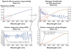
A fundamental disadvantage exists with using halogen sources to test silicon sensors—that is, the spectral power distribution of a halogen source is quite low in the UV and deep blue region. Coincidentally, that is also where the sensitivity curve of silicon is lowest. These two factors combine in any application where halogen sources are used to characterize silicon CCD and CMOS sensors, and lead to a poor signal-to-noise ratio (SNR). On the other hand, blue LED emitters are among the most efficient of any LED color.
To get around the low amount of energy in the blue, conventional optical filtering techniques may be used. However, filtering light or using monochromators is a subtractive method, meaning that it will never produce more energy out than is put in. Therefore, even if the relative blue content of a halogen lamp is increased using a “daylight” filter, the overall power will be limited. In comparison, the TLS approach uses different color LEDs in an additive method, combining different LEDs and adding power just where it is needed for a given spectral output.
Figure 3 illustrates this point in greater detail. A blackbody curve and silicon response curve are shown, and the resulting raw signal is indicated. The same comparison is done with a LED source generating a high correlated color temperature (CCT) output—in this case, the result is flat across the spectrum. In this fashion, the SNR across the entire wavelength range can be made essentially flat. The result is a more accurate representation of the true SNR across all wavelengths, without a bias towards the near-infrared. In general, this means any type of test that may be performance-limited will have better signal fidelity in the blue region.Sensor frame rate and readout time
One major area of advancement in sensor development is in readout speed and overall frame rate. High-speed cameras are becoming more popular in a variety of applications, but maintaining speed as pixel counts skyrocket can be challenging. Main drivers for overall frame drive rate start at a purely electrical level with the serial conversion time (the time required to digitize a single pixel), the overall number of pixel rows and columns, and the time required to clear the charge from registers. However, in full camera assemblies, other factors exist such as the exposure time required for a given capture and the delay from mechanical shutters opening and closing.
Taking all those factors into account gives a close estimate of the theoretical frame rate, but actual performance needs to be verified using a physical standard. This often requires a light source to be modulated with frequencies on the same order of magnitude as the frame rate. High-quality TLS devices provide pure DC current drivers that avoid high-frequency pulse-width modulation flicker that can create undesirable effects in the measurement. However, the ability to modulate the drive current on millisecond timescales can be useful to fully characterize the electronic readout time or the overall frame rate.
Just as the majority of commercial, residential, and automotive lighting has moved to solid-state LEDs, so too will LEDs eventually surpass traditional lighting for scientific and industrial applications. While there have been some technological roadblocks with stability and repeatability of early LED sources, new advancements have allowed LED performance to be refined so that it is suitable for scientific measurements. These advances have allowed LED-based tunable sources to be used for nearly any image sensor characterization method.
In many areas, TLS capabilities surpass traditional halogen-based methods for these measurements in terms of stability, performance, and speed. New TLS devices can also replace multiple pieces of legacy equipment, as there is much more versatility and flexibility in how the output can be tuned and adapted for a variety of tests. In addition, overall operational lifetime of the LEDs is more than 100X longer than halogen lamps, with high stability and faster switching time. Nearly any image sensor test procedure can be improved and optimized using new LED tunable light source technology.

Trevor Vogt | Director of Engineering
Trevor Vogt is the Director of Engineering for Gamma Scientific, joining the company in 2011. He is a native Californian and graduated with an Electrical Engineering degree from the University of California, Santa Cruz. Mr. Vogt currently leads the Research and Development function for Gamma Scientific, pursuing new technologies and product designs for a wide variety of optical metrology applications. His technical expertise includes thin film optical coating metrology, camera and sensor design, optical metrology, spectrometry & spectroradiometry, LED / lighting test and characterization and industrial automation. He has several publications in the area of light measurement and optical sensing.


