Photodiodes: Dynamic photodiodes reach single-photon sensitivity at low voltages, with minimal noise
MAXIM GUREEV and DENIS SALLIN
Standard photodiodes operate at constant reverse bias. The incident light intensity is converted into an electrical current that is typically weak and requires amplification. The amplifiers consume power and silicon area, have limited bandwidth, and introduce additional noise. That’s why in applications requiring fast measurement of weak light signals, like time-of-flight 3D sensing, detectors with internal gain are used. These detectors, such as avalanche photodiodes (APDs) and single-photon avalanche diodes (SPADs), use impact ionization mechanisms to amplify the signal. Unfortunately, this mechanism requires high voltage, which makes the integration of these detectors into mobile devices complex and expensive.
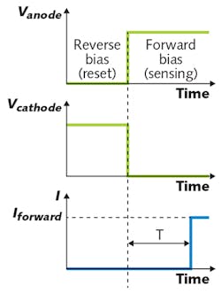
ActLight’s dynamic photodiode (DPD) uses a new operating mode that converts light intensity into time.1-3 The applied voltage is not constant, but is switched from reverse to forward bias. Applied forward bias induces a large forward current that doesn’t start immediately, but after a time delay (see Fig. 1). The forward current magnitude is controlled only by the applied voltage, and its value does not depend on the light intensity. In contrast, the delay time (triggering time) is a function of the absorbed light power.
The high amplitude of the output signal allows direct integration of the DPD with digital circuits, without any analog amplification. As a result, there is no additional noise in the system and the detector is shot-noise limited over the whole range of light intensities. At the same time, the ActLight DPD operates at voltages of around 1 V and can be manufactured with standard complementary metal-oxide semiconductor (CMOS) technologies.
With CMOS compatibility, a high-amplitude output signal, low noise, and low voltage operation, the DPD can also be tuned to reach single-photon sensitivity. This could dramatically enhance the performance of wearable devices and smartphones.
Light-dependent operation
The behavior of the DPD can be described as follows: the photocurrent charges the internal capacitor of the device and as soon as a certain critical charge Qcrit is accumulated, the device triggers and a strong forward current flows. For higher light intensities, the capacitor charges faster and the triggering time is shorter. The triggering time Ttrig is inversely proportional to light intensity Ilight through the equation Ttrig = Qcrit/(A*R*Ilight + idark), where idark is the dark current, A is the active area, and R is the responsivity.
The critical charge depends on the device geometry and bias voltage and can be adjusted to optimize DPD performance for the particular application—that is, the physical device can be tuned to set Qcrit, from 107 electrons down to 1.
In darkness, triggering times in the 100 ms range can be reached. For high intensities, sub-nanosecond triggering times are possible. Hence, the DPD has an extremely high dynamic range, limited by dark current on the low-light side and by the resolution of the time-to-digital converter (TDC) on the strong-light side.
Wearable device applications
In the last few years, the number of wearable devices used for health monitoring and sport/fitness tracking has increased exponentially. These devices require accurate, low power, and affordable vital-sign sensors. Photoplethysmography (PPG) is a technology of choice for wearable devices, enabling the monitoring of vital signs such as heart rate, blood oxygen saturation (SpO2), and blood pressure.
In PPG sensors, the light emitted by LEDs and reflected from human tissue is measured with a photodiode. The reflected signal depends on the blood concentration in the tissue. With each cardiac cycle, heart pumps blood, changing absorption and, consequently, the light intensity at the photodiode. The modulation of the photodiode signal gives information about vital signs. This modulation is typically small (0.1–1%), and a good signal-to-noise ratio (SNR) is essential to provide reliable data.
Most commercially available PPG systems include a standard photodiode and analog front end (AFE; see Fig. 2). The AFE is the main source of noise, and the LED power should be relatively high to provide the required SNR. This AFE is also responsible for the main part of the overall power consumption of the system.In the case of PPG systems based on DPDs with a TDC, light is converted directly into a digital signal, avoiding the need for an area- and power-consuming analog front end. The fully digital circuits allow complete removal of the noise associated with the analog signal chain, meaning that less light is needed to achieve the same SNR. The LED power consumption can be significantly reduced, improving the autonomy of battery-powered devices. The size of the photodetector can also be reduced, which is critical for PPG applications for wearables.
TOF sensing applications
The high SNR provided by the DPD architecture is also beneficial for time of flight (ToF) 3D sensing. Basic ToF systems consist of a light source (laser or LED) and a detector—time of light propagation from the source to the object and back to the detector is measured, providing the distance information.
There are two main ToF methods: direct ToF (dToF) and indirect ToF (iToF). In dToF, the time of arrival of the reflected light pulse is measured directly. In principle, one measurement is enough to measure distance, while in practice thousands of measurements are used to get acceptable precision. In iToF, several measurements are required to measure distance. The most common iToF method is based on locked-in-pixel methods, requiring customized technology.4-5
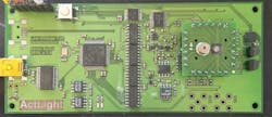
Alternatively, ActLight developed an iToF method using its DPD that can be manufactured with a standard CMOS or CMOS Image Sensor (CIS) process. The low-voltage iToF range meter demonstrator allows measurement at distances up to 5 m in a wide range of lighting conditions (see Fig. 3). Furthermore, it has demonstrated full sun (>100 klux) background light immunity.Leveraging single-photon sensitivity
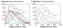
With the development of 3D sensing ToF technologies (especially for smartphones) where the amount of light available for sensing is extremely limited, detectors with single-photon sensitivity attract a lot of attention. ActLight has optimized its DPD to reduce the internal capacitance and, consequently, the critical charge (see Fig. 4). The statistical distribution (histogram) of triggering time for different values of bias voltage corresponding to the critical charge equal to 1, 2, 3, 5, and 7 electrons are in good agreement with theoretical distributions obtained for integrating devices where charge accumulation can be described as a Markov process. Here, the Poisson distribution of electrons is assumed.The remarkable feature that can be seen on both theoretical and experimental histograms is the abrupt change of the distribution form when the DPD changes from two-photon to single-photon sensitivity—essentially, this transition proves the ability to reach single-photon sensitivity. This exponential statistical distribution is a feature of single-photon detectors, equivalent to the statistical distribution observed in SPADs.
Moreover, the general behavior of a DPD with single-photon sensitivity is identical to a SPAD. As soon as a single electron reaches the device, a strong output signal is generated. The device is then switched into reset mode, and then to sensing mode. It can be considered as a direct low-voltage replacement of a SPAD in existing systems. For example, in direct ToF systems, a SPAD can be replaced by a DPD without changing the measurement principles and circuits.
Low-voltage operation is exceptionally important in portable applications where power-hungry and area-consuming circuits like charge pump are used to generate high voltage. The problem of high-voltage generation is especially critical for 3D cameras that need to power an array of pixels. The low voltage is also favorable for pixel scaling because of the absence of a high electric field between pixels.
Tunability of a DPD, accomplished by changing the number of electrons needed for triggering by changing the applied voltage, can be used to increase the dynamic range and background light immunity of the DPD. Potentially, it can help avoid a macropixel architecture, radically reduce the pixel size, and serve a number of other portable sensing applications that increasingly depend on device miniaturization.
REFERENCES
1. S. Okhonin et al., Appl. Phys. Lett., 106, 031115 (2015).
2. S. Okhonin, “Photo detector and methods of manufacturing and operating same,” U.S. patent 9,012,960 B2 (2015).
3. S. Okhonin et al., “Photo detector systems and methods of operating same,” U.S. patent 9,735,304 B1 (2017).
4. R. Lange, “3D time-of-flight distance measurement with custom solid-state image sensors in CMOS/CCD-technology, dissertation,” University of Siegen, (2000); http://bit.ly/photodiodesref4.
5. B. Büttgen, et al., “CCD/CMOS lock-in pixel for range imaging: Challenges, limitations and state-of-the-art,” Proceedings of the 1st Range Imaging Research Day, ETH Zurich (Sep. 2005).
Maxim Gureev is chief technology officer and Denis Sallin is director of engineering, both at ActLight, Lausanne, Switzerland; e-mail: [email protected]; www.act-light.com.


