Photonics Applied: Quantum Photonics: UNIQORN—Making quantum photonics affordable
Whereas the first quantum revolution led to the development of devices like lasers, semiconductors, transistors, and other devices that follow the laws of quantum mechanics, the second quantum revolution promises completely novel approaches to information processing that can outperform classical implementations in the fields of computing, cryptography, and sensing technologies.
Efforts are currently underway to transform laboratory demonstrations into actual prototypes and products. Especially in quantum communications, which includes technologies like quantum key distribution (QKD), quantum random number generators (QRNGs), and entangled photon sources for future quantum repeater networks, applications have already successfully passed field-trial stage and are slowly entering the marketplace.1, 2
However, the realization of setups that can produce, manipulate, and measure single quantum states is expensive, and more importantly, rather bulky and fragile due to the implementation in free-space optics. Within the UNIQORN project, 17 partners are driving the second quantum revolution by merging quantum communications with photonic integration technology in the framework of the European Quantum Flagship.3
One of the goals of the UNIQORN project is the miniaturization of laboratory-proven QKD and other quantum communications setups by combining photonic integration with free-space optics via a newly developed on-chip micro-optical bench in a PolyBoard platform. The aim is room-temperature-compatible, low-cost, and small-footprint pluggable devices that can make quantum technologies available for everyone.
A micro-optical PolyBoard bench
Developed by the Fraunhofer Heinrich Hertz Institute (Fraunhofer HHI; Berlin, Germany), the PolyBoard integration platform allows for the hybrid integration of a multitude of photonic functionalities on a single chiplet for applications ranging from classical fiber-optic communications to sensing and spectroscopy as well as life sciences.
The platform consists of passive polymer single-mode waveguides complemented by additional building blocks like optical couplers and switches, arrayed waveguide gratings (AWGs), thin-film elements (TFEs) for polarization and wavelength handling, as well as variable optical attenuators. End-face coupling and micromachined 45° mirrors allow for the low-loss integration of active elements such as gain chips, laser diodes, and photodetectors.4 Furthermore, the addition of graphene layers enables electro-absorption modulators inside the passive polymer waveguides.5
Recently, the first PolyBoard-based optical isolator using on-chip and free-space technology was successfully demonstrated.6 The micro-optical bench technology in PolyBoard not only allows for the integration of magneto-optical materials, but virtually anything ranging from crystals to fluids or just air. Particularly, the ability to support polarization diversity, nonlinear optical media, and single-photon detectors on a single chip greatly enhances the spectrum of possible quantum applications. This diversity displays the strength of the PolyBoard over other integration platforms like indium phosphide (InP), silica nitride (Si3N4), or silicon-on-insulator (SOI), since those platforms can only support a much narrower range of electro-optical functionalities.
Within UNIQORN, the PolyBoard concept will be applied to the integration of nonlinear optical crystals such as potassium titanyl phosphate (KTP) or lithium niobate (LiNbO3) to use effects like spontaneous parametric down conversion (SPDC) or second-harmonic generation (SHG) to generate entangled photon pairs. In fact, the micro-optical bench has already proven its effectiveness as a key building block for the on-chip integration of nonlinear optical crystals in PolyBoard.
Early integration success
Recently, UNIQORN demonstrated on-chip integration of an optical isolator. Optical isolators and circulators are two of the most challenging optical functionalities for photonic integrated circuits (PICs) because they rely on non-reciprocal optical effects. So far, attempts to integrate magneto-optical materials into existing photonic platforms have not moved beyond the R&D laboratory stage—mostly due to the high insertion losses of the fabricated devices.
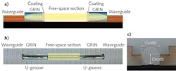
Fraunhofer HHI has succeeded in demonstrating the first integrated optical isolator on its PolyBoard platform. This hybridly integrated isolator consists of two polarization filters and a Faraday rotator from pre-magnetized bismuth-doped yttrium iron garnet. The micro-optical bench comprises of a pair of graded-index (GRIN) lenses that are inserted into pre-etched U-grooves and butt-coupled to polymer-based single-mode waveguides. Both lenses create an on-chip free-space section between the endfaces in which a collimated beam propagates.
Due to the tight tolerances of the lithographic definition of the U-grooves, the PolyBoard allows for direct passive coupling of the GRIN lenses to the polymer waveguides without the need for further active alignment. This concept was originally developed for purely passive fiber-to-chip coupling, with coupling losses below 0.1 dB (see Fig. 1).
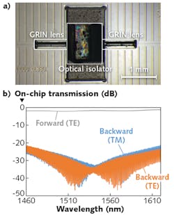
This free-space architecture enables the integration of additional optical functionalities—for example, an isolator consisting of two polarization filters and a 45° Faraday rotator (see Fig. 2). The optical beam in the free-space section is collimated by both GRIN lenses. This minimizes the optical transmission losses through the magneto-optic crystal that are normally incurred by the divergence of the unguided light if the crystal were to be coupled directly to the single-mode waveguides.Waveguide-to waveguide loss of such an optical isolator in the PolyBoard platform is as low as 1.4 dB. An optical isolation of >20 dB over a bandwidth of 150 nm with a peak isolation of >30 dB at a compact footprint of less than 3 × 1 mm demonstrates the ability of the micro-optical bench to combine the advantages of integrated and free-space optics on a single chip.
Quantum-systems-on-chip methodology
For the first time, UNIQORN accommodates nonlinear optical materials such as KTP or LiNbO3 in complex photonic integrated circuits. In those materials, SPDC occurs and a high-energy pump photon decays into two low-energy photons. Currently, SPDC is the cleanest way to produce photon pairs and entanglement with the highest purity and is widely used in quantum optics experiments.7
To make full use of these nonlinear optical effects on the chip, wavelengths beyond the classical fiber-optic communications wavelengths are required. The wavelengths utilized in UNIQORN span from 500 nm in the visible up to 1650 nm in the near-infrared. This also requires an integration platform that is transparent and allows for filtering and on-chip routing across all these wavelength bands. In contrast to most other photonic integration platforms, PolyBoard meets this fundamental requirement.
The PolyBoard-based optical engines that will be developed in the UNIQORN project include a polarization-entangled photon source and a squeezed-light generator (see Fig. 3).Based on an integrated periodically poled KTP crystal, the polarization-entangled photon source features TFEs for efficient wavelength and polarization handling. The KTP crystal is inserted into a free-space section and generates photon pairs at wavelengths of 760 nm and 1550 nm via SPDC using a pump source at 510 nm. By careful selection of the phase-matching conditions, two SPDC processes with orthogonal polarization modes (horizontal and vertical) can be supported by the KTP crystal, resulting in a polarization entangled state.8 While the entangled photon at 1550 nm is transmitted to a corresponding PolyBoard receiver via a standard single-mode fiber, the polarization state of the photon at 760 nm is measured on chip by a combination of polarization-handling TFEs and an array of silicon-based single-photon avalanche detectors (SPADs) that are butt-coupled to the polymer waveguides at the chip edge.
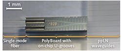
The two-mode squeezed-light vacuum engine is based on the integration of waveguide-inscribed periodically poled lithium niobate (ppLN) crystals into the PolyBoard. Together with an InP-based gain element, the lower ppLN crystal acts as a 775 nm SHG pump source for the ppLN crystal. The latter acts as a double resonant cavity to create squeezed states of light in amplitude and phase. In preliminary tests, successful coupling of ppLN waveguides to polymer waveguides was achieved for both PolyBoard optical engine designs (see Fig. 4).Another quantum engine implemented on the PolyBoard is a quantum random number generator, whose randomness is derived directly from the random measurement outcomes inherent in the theory of quantum mechanics. The PolyBoard provides the platform for a laser that injects single photons that are then split by an integrated beamsplitter and detected by SPADs on the chip. Since photons are not divisible, a photon can only be found in one of the output ports of the beamsplitter and hence, its detection provides a random bit.
UNIQORN will also address the distribution of entangled photons needed for future quantum repeater networks. Combining a variant of the entangled photon source described previously, but with both photons having a wavelength around 1550 nm, together with space switches on the PolyBoard, an entanglement distribution node is created that can actively route entanglement to different users in an optical network.9
In contrast to other quantum technology solutions that require cryogenic temperatures, UNIQORN quantum-systems-on-chip operate at room temperature and above. This is compatible with widely used standard thermoelectric coolers, increases energy efficiency of the quantum system, and minimizes system footprint, eliminating major obstacles to the acceptance and market penetration of quantum technologies in optical communications.
ACKNOWLEDGEMENTS
The UNIQORN project receives funding from the European Union’s Horizon 2020 research and innovation program under grant agreement No. 820474. The ppLN waveguide samples were provided by professors Christine Silberhorn and Harald Herrmann from Universität Paderborn (Paderborn, Germany).
REFERENCES
Please see https://bit.ly/apr19references.
Moritz Kleinert | Project Manager, Fraunhofer HHI
Moritz Kleinert is a Project Manager at the Fraunhofer Heinrich Hertz Institute (Fraunhofer HHI; Berlin, Germany).
Hauke Conradi | Research Associate, Fraunhofer HHI
Hauke Conradi is a research associate at the Fraunhofer Heinrich Hertz Institute (Fraunhofer HHI; Berlin, Germany).
Bernhard Schrenk | Senior Scientist, AIT Austrian Institute of Technology
Bernhard Schrenk is a senior scientist at the AIT Austrian Institute of Technology (Vienna, Austria).
Hannes Hübel | Scientist, AIT Austrian Institute of Technology
Hannes Hübel is a scientist at the AIT Austrian Institute of Technology (Vienna, Austria).


