Leica Microsystems opens dedicated microscopy lab in Japan

April 17, 2014
Leica Microsystems has opened a laboratory in Tokyo, Japan, dedicated to product demonstrations of the company's microscopy systems and workshops.

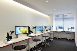
Leica Microsystems (Wetzlar, Germany) has opened a laboratory in Tokyo, Japan, dedicated to product demonstrations of the company's microscopy systems and workshops. The lab—dubbed the Experience Lab—also serves as a showroom for microscopy users who wish to familiarize themselves with instruments and accessories such as cameras, illumination, and software. Users are free to bring their own samples to observe with the systems and can also take advantage of a sample preparation service.

Related: 3D-enabled Leica Microsystems microscope performs ophthalmic surgery

Takashi Ueno, president of Leica Microsystems KK in Tokyo, explains that the new lab also has onsite application specialists available to answer questions, give advice, and offer training on the company's imaging systems.

The lab, located in the company's Tokyo office, is equipped with microscopy systems for clinical, life science, and industrial applications. For more information, please visit https://xlab.leica-microsystems.com.
Sponsored Recommendations

Hexapod 6-DOF Active Optical Alignment Micro-Robots - Enablers for Advanced Camera Manufacturing

Dec. 18, 2024
Optics and camera manufacturing benefits from the flexibility of 6-Axis hexapod active optical alignment robots and advanced motion control software

Laser Assisted Wafer Slicing with 3DOF Motion Stages

Dec. 18, 2024
Granite-based high-performance 3-DOF air bearing nanopositioning stages provide ultra-high accuracy and reliability in semiconductor & laser processing applications.

Free Space Optical Communication

Dec. 18, 2024
Fast Steering Mirrors (FSM) provide fine steering precision to support the Future of Laser Based Communication with LEO Satellites

White Paper: Improving Photonic Alignment

Dec. 18, 2024
Discover how PI's FMPA Photonic Alignment Technology revolutionized the photonics industry, enabling faster and more economical testing at the wafer level. By reducing alignment...

Voice your opinion!

To join the conversation, and become an exclusive member of Laser Focus World, create an account today!