FEMTOSECOND LASERS/OPTICAL MICROSYSTEMS: 3D printing of medical microsystems with ultrafast lasers
ERIC MOTTAY and YVES BELLOUARD
The use of microsystems in life sciences is vast and growing, with applications ranging from basic research to diagnostics and therapeutics. Ultrafast lasers enable a radically different and alternative approach to traditional microsystems manufacture. In doing, they also meet increasing demands for smaller structures (typically on the order of a few millimeters) with submicron features integrated into the active elements and multifunctionality involving simultaneous integration of mechanical, electrical, fluidic, and optical components.
Rather than building a device by combining and assembling different materials and functions, ultrafast lasers turn a single piece of material into a microsystem by locally modifying its properties. The distinction between substrate, component, function, or device is lost and costs and manufacturing complications are substantially reduced.
Fused silica
Microdevices manufactured with ultrafast lasers use glass or silica as the main component—not silicon, as in traditional microsystems. A perfect material for optical functions, fused silica is a less intuitive candidate for mechanical functions. However, it has excellent mechanical properties at the microscale, provided that its surface properties are well controlled.
Manufacturing of fused silica microdevices is a two-step process, somewhat similar in principle to photography. During the first step, the bulk silica is exposed to laser power low enough to produce no observable change in material structure but high enough to induce local densification of the fused silica.
In the second step, the substrate is etched in a low concentration hydrofluoric acid solution. The etching rate is much higher for the densified part of the material, leading to preferential etching of the laser-exposed volume. This laser-exposed zone is typically etched 100 times faster than the pristine material.
It then becomes straightforward to design and manufacture many different mechanical and fluidic components by carefully controlling the shape of the laser-exposed area.
Because the laser is altering material properties instead of removing material, it has specific requirements different from what is usually needed in laser ablation and micromachining processes. The process is conducted below the ablation threshold and the pulse energy is typically a few tens of nanojoules to a microjoule. The pulse repetition rate goes from a few hundred kilohertz to several megahertz. It should be noted that for high laser speeds above 1 MHz, cumulative heat absorption in the fused silica may influence the exposure process. Finally, pulse duration is between 150 and 500 fs.
FemtoPrinter
The low energy required for laser exposure of silica enables the use of ultra-compact, air-cooled ultrafast lasers, which can be integrated in a 3D printing system. The FemtoPrint research project (www.femtoprint.eu), sponsored by the European Union, brought together leading academic institutions and industrial companies to develop such a printer.
Consisting of a shoebox-size ultrafast laser (see Fig. 1a), advanced beam handling and focusing, and user-friendly control software, the FemtoPrinter (see Fig. 1b) can produce three-dimensional (3D) patterns with nanoscale features in glass. Following the research project, the start-up company FemtoPrint was launched to commercialize the 3D microprinter.
The FemtoPrinter has the unique capability to perform multifunctional manipulation on a single substrate of glass or silica, allowing the fabrication of several key functions on the device: Micromechanical components, fluidic channels, optical waveguides, and sensors.
Flexures, channels, and waveguides
Flexures are mechanical elements commonly used in precision and microengineering to precisely guide mechanical motion. They deform elastically and are far less sensitive to friction, wear, and hysteresis than traditional multi-part components. In spite of the brittleness of glass and fused silica at macro-scale, flexures with a strength up to 3 gigapascal (GPa) have been demonstrated (see Fig. 2a).
Flexures are essential building blocks for more complex micromechanical components. For example, a comb array etched in glass and coated with a transparent ITO electrode makes possible a totally transparent microactuator. This enables the combination of mechanical micromanipulation with direct optical sensing, unhindered by any opaque structure.
The fabrication of high-aspect-ratio, arbitrary-shape fluidic channels is also a key feature of this process (see Fig. 2b). The flexibility in initial 3D laser exposure enables the option to scribe surface channels, or volume tunnels integrated in the substrate. There is virtually no limit on the aspect ratio achievable. Millimeter-long structures with diameters of 10 μm are routinely achieved. These channels, too, are key for microfluidic systems.
Finally, the laser exposure induces a change in the refractive index of the substrate, creating optical waveguides within the substrate without any additional materials, which can then be integrated into optical sensors. The 3D printing process even enables the manufacturing of curved waveguides.
Result: Real-time water analysis
Researchers at Technical University Eindhoven have demonstrated an example of a complete microsystem manufactured with this ultrafast laser-based process: It consists of a biochip designed for fast screening, real-time monitoring, and initial classification of algae (see Fig. 3). Rapid identification of algae species is a valuable tool to assess water quality and monitor adverse events such as eutrophication, or the phytoplankton "bloom" in response to an increase in nutrients, such as nitrate or phosphates.
At present, identifying the algae content in a water sample requires the specimen to be transported to a laboratory and specific tests conducted in a specialized environment by trained personnel. Microfluidic devices manufactured using ultrafast lasers offer an inexpensive alternative with the added value of on-site detection and monitoring of microorganisms. This capability not only allows for rapid threat assessment and reaction times, but also gives rise to the possibility to down-skill the measurement process, further reducing costs. These devices are compact, portable, and can perform real-time analysis. Only ultrafast laser technology offers the possibility to manufacture such a small, multifunctional device.
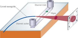
The sensor incorporates both fluidics and optical functions. A square channel, with a cross-section of 100 × 100 μm, is exposed and then etched in the glass. A 90° curved waveguide is realized, perpendicular to the surface of the channel. The curvature of the waveguide eliminates uncoupled, parasitic light. The radius of curvature is 18 mm, determined by the laser-induced refractive index change.
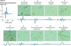
The water sample flows inside the fluidic channel. A fiber-coupled laser source is launched into the optical waveguide, illuminating a section of the channel. The transmitted light is then analyzed with a four quadrant photodetector. If a cell or particle flows into a channel, it casts a shadow on the photodetector. The composite signal from the four quadrants will be characteristic of the shape of the particle going through the channel (see image at top of this page). Software processing then correlates the signal with a specific algae species for identification. Experimental results have demonstrated that nine different species of algae flowing into the same channel can be identified, with an accuracy of 85%.
Further development is possible on the sensor: Adding other waveguides may lead to more quantitative information such as flow rate and additional data on algae geometry. Integration of external functions (flow handling, beam detection) on the device will further reduce its size and increase its flexibility.
Meeting future needs
As microsystems become more advanced and demand multifunctional capabilities for life sciences applications, ultrafast laser technology is stepping up to meet these needs, enabling fabrication of arbitrary-shaped channels (surface scribes and volume tunnels integrated in the substrate) and virtually no limit on the aspect ratio achievable on a single substrate.
Eric Mottay is president and CEO of Amplitude Systemes (Pessac, France; www.amplitude-systemes.com), and Yves Bellouard, Ph.D., is Associate Professor in Micro-/Nano-Scale Engineering at the Mechanical Engineering Department of Eindhoven University of Technology (The Netherlands; www.tue.nl/en). Contact Mr. Mottay at [email protected].


