Photonics Applied: Biometric Security: The second wave of consumer biometrics is reshaping the VCSEL industry
GUILLAUME GIRARDIN and SYLVAIN HALLEREAU
Fingerprint identification was the first biometric technology used for consumers mainly for historical reasons, beginning with the criminal fingerprint database established by the U.S. Federal Bureau of Investigation (FBI) in 1892 using ink-based techniques. In 2013, it entered mass-adoption status, thanks to Apple’s (Cupertino, CA) introduction of Touch ID on the iPhone 5s. Since then, fingerprint sensing has remained the most common biometric technology currently used in the consumer space—but probably not for long.
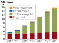
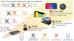
Yole Développement (Yole) estimates that the annual revenue generated by fingerprint-based hardware solutions for the consumer market is currently $2.7 billion, representing 57% of the total consumer biometric hardware market ($4.8 billion in 2018).
Like fingerprint detection, 3D facial recognition meets almost all the requirements of a “perfect” biometric recognition technology: it is robust, stable and repeatable, almost time invariant when compensated by artificial intelligence (AI) algorithms, difficult to spoof, is “unique” amongst a population, accessible, easy to use, and acceptably nonintrusive, even if some concerns have arisen.
Biometry’s second wave
Well anticipated by Yole in mid-2016, this second wave of biometrics has gained huge momentum since the end of 2017, thanks to the same player as fingerprint sensing technology in 2013—namely Apple, but with the iPhone X. A biometric 3D facial recognition feature has been made possible because of the integration of a specific type of 3D sensing module called structured-light 3D sensing (as opposed to stereo and time-of-flight approaches detection), based on the former work by PrimeSense, which was acquired by Apple in 2013.
With the introduction of 3D facial recognition, Apple has also set the technology and use-case standard for 3D sensing in the consumer market. Apple designed a complex assembly of camera modules and vertical-cavity surface-emitting laser (VCSEL) light sources using structured-light principles, along with a near-infrared (near-IR) global shutter image sensor from STMicroelectronics (Geneva, Switzerland) to perform secure 3D facial recognition.
This second wave of biometry using costly technology will therefore push the market value toward $15 billion by 2023. As a direct consequence, 2018 will be the last year in which fingerprint sensing dominates biometric technologies (see Fig. 1).
Despite a major slowdown of the smartphone industry, Yole still expects a good penetration rate for 3D facial recognition. While players must innovate and offer the best smartphone features to take market from the competition, all major Chinese players (Huawei, Oppo, Vivo, Xiaomi) have embraced 3D facial recognition, growing the 3D sensing hardware market from $1.5 billion in 2018 to $11.5 billion by 2023 (see Fig. 2).3D facial recognition is based on a structured-light detection approach that requires various critical miniaturized components—in particular, VCSELs and diffractive optical elements (DOEs). These DOEs are used to project a pattern onto a scene that is then reconstructed into a 3D map. The DOE diffracts the coherent light ray coming from the VCSEL to project a special pattern. By analyzing the deformation of this pattern from the scene, the algorithms and IR cameras can then reconstruct the scene in three dimensions. The VCSEL is thus a critical component that is disrupting the biometrics market.
The VCSEL boom
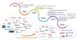
Since its demonstration in 1979, the VCSEL has penetrated multiple applications and changed the scale and scope of several markets (see Fig. 3). Optical data communication was the first industrial application to start integrating VCSELs. With lower power consumption and a competitive price compared to edge-emitting lasers (EELs), VCSELs have flourished in data applications and now, sales are being driven by the development of datacenters since the 2000s. Some new applications for VCSELs have emerged, such as for laser printers and optical mice, but these are not high-dollar markets.In 2014, almost 20 years since the first use of the technology in datacom, VCSELs started to make their way into high-volume consumer smartphones. They were first coupled with sensors for proximity sensing and autofocus functions and therefore began their rise in 3D sensing applications. The iPhone X, released in 2017, integrates three different VCSEL dies for the proximity sensor and the facial ID module, triggering an explosion in the VCSEL market and propelling overall revenue to around $330 million.
Good iPhone X sales in late 2017 and early 2018 have piqued the interest of other smartphone brands in VCSEL-based 3D sensing functions. Less than one year after the release of Apple’s flagship, its competitors are now following the same trend and are starting to integrate 3D sensing technologies. Xiaomi and Oppo were the quickest, with the Xiaomi Mi8 and the Oppo Find X models released in the second quarter of 2018. Other leading smartphone players, such as Huawei, Vivo, and Samsung, are also expected to integrate VCSELs into their flagship models by 2019.
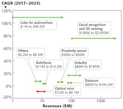
In this context, the explosion of VCSEL demand that was initiated in 2017 will persist for the next five years, potentially multiplying the business opportunity more than tenfold. During this time, the technology might also find some new growth drivers in automotive light detection and ranging (lidar) or gas sensors, further fueling the VCSEL industry in coming years in the form of investment, new entrants, and mergers and acquisitions (see Fig. 4).Reverse engineering discoveries
The strategic analyses developed by Yole’s team are complemented by the technical expertise of its partner, System Plus Consulting. Over the years, System Plus Consulting has developed reverse engineering and costing expertise for semiconductor products, analyzing more than eight smartphones and systems with VCSELs for 3D recognition or time-of-flight (TOF) sensing.
Depending on the application, function, or light power, the surface area of the VCSEL ranges from a nominal 0.02 mm2 for TOF proximity sensing to more than 4 mm2 for gesture-recognition sensing at distances up to 4 m. For smartphone applications, especially for facial recognition, the VCSEL area is typically between 0.5 and 2 mm2.
Based on its analysis of these smartphone systems, System Plus Consulting has identified the technologies and the manufacturers of the different VCSELs that can be found on several flagship models in the market, providing a deep understanding of the technology choices for leading original equipment manufacturers (OEMs).
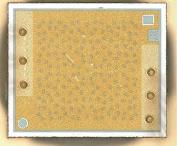
Apple, the first company to integrate a structured-light system in its flagship iPhone X, took the choice of having two high-end components: first, a dot projector, using complex wafer-level optics and gratings, from ams/Heptagon (Graz, Austria) coupled with a Lumentum (Milpitas, CA) VCSEL array featuring 320 cavities randomly distributed (see Fig. 5); and second, a custom near-IR sensor using a silicon-on-insulator (SOI) substrate.Xiaomi (Beijing, China) made a simpler choice for its Mi 8 Explorer Edition by combining a market-available near-IR camera sensor with a mask-based dot projector using a camera module with an array-patterned mask occluding the VCSEL emission from Princeton Optronics (Trenton, NJ) 2 mm2 VCSEL showing more than 950 VCSEL cavities. The Princeton Optronics VCSEL has a more complex distributed Bragg reflector (DBR) with 20% more layers than the Lumentum VCSEL DBR design, but both VCSELs use lateral oxidation for the aperture of the cavities.
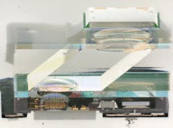
Oppo (Dongguan, China), for the Find X, took a similar direction as Xiaomi. While featuring the same camera module configuration, the dot projector is slightly different, using lens diffraction instead of a mask pattern (see Fig. 6). Indeed, every OEM has made a choice of one component that changes the whole system: dot patterning, coded pattern, or digital algorithm.Completing the facial recognition system, all OEMs chose a different camera. High-end OEMs like Apple have chosen the near-IR sensor developed by STMicroelectronics. Based on a SOI substrate supplied by Soitec (Bernin, France), the sensor uses front-side illumination (FSI) featuring 1.5M pixels in a 30 mm2 die area. Chinese companies like Xiaomi, Oppo, and Huawei have chosen to integrate a near-IR sensor from OmniVision (Santa Clara, CA), also using FSI and featuring 1.07M pixels in a 20 mm2 square die area.
The configurations and approaches developed for 3D facial recognition modules are based on a complex assembly of state-of-the-art technologies and components. This has led to manufacturing and supply chain challenges that are quite hard to manage by the OEMs and therefore a key aspect to competition. Low yields in the manufacturing of 3D sensing modules has led to heightened cost and has driven huge increases in component volumes, further driving investment and M&A activity. Innovation and big money remain key assets to stay in the race for those gigantic consumer markets.
Guillaume Girardin is director of the Photonics, Sensing & Display Division at Yole Développement, part of Yole Group of Companies, Lyon-Villeurbanne, France; e-mail: [email protected]; www.yole.fr, while Sylvain Hallereau is project manager at System Plus Consulting, part of the Yole Group of Companies, Nantes, France; www.systemplus.fr.
