Room-temperature low-excess-noise APDs are InP-compatible for lidar applications

Avalanche photodiodes (APDs) operating at 1550 nm wavelengths struggle to operate with very high sensitivity and high speed due to the material properties of the indium phosphide (InP) or indium aluminum arsenide (InAlAs) that is typically used as the avalanche gain medium. The stochastic nature of the impact ionization process leads to excess noise and the multiple electron transits required to achieve high gain degrade the speed of these APDs.
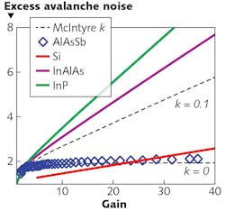
Recent work at the Universities of Cardiff and Sheffield in the UK as well as the University of California, Los Angeles (UCLA) has shown that the alloy aluminum arsenide antimonide (AlAsSb) grown lattice-matched to InP has very different electron and hole ionization coefficients that enable extremely low excess avalanche noise. This enables highly sensitive telecommunication wavelength APDs on a standard InP photonics platform and high-speed devices, even when operating at high gain due to the extremely small hole ionization behavior.
Simulations of an InGaAs-AlAsSb-based APD suggest that a sensitivity of -25.7 dBm at 25 Gbit/s with a bit-error-rate of 10-12 should be achievable and with a bandgap of 1.55 eV at room temperature. John David of the Advanced Detector Centre in Sheffield says, “High-sensitivity, high-speed APDs operating at 1550 nm will be a key component in lidar systems for autonomous vehicles and for other sensing applications.” Reference: X. Yi et al., Nat. Photonics (2019); https://www.nature.com/articles/s41566-019-0477-4.

Gail Overton | Senior Editor (2004-2020)
Gail has more than 30 years of engineering, marketing, product management, and editorial experience in the photonics and optical communications industry. Before joining the staff at Laser Focus World in 2004, she held many product management and product marketing roles in the fiber-optics industry, most notably at Hughes (El Segundo, CA), GTE Labs (Waltham, MA), Corning (Corning, NY), Photon Kinetics (Beaverton, OR), and Newport Corporation (Irvine, CA). During her marketing career, Gail published articles in WDM Solutions and Sensors magazine and traveled internationally to conduct product and sales training. Gail received her BS degree in physics, with an emphasis in optics, from San Diego State University in San Diego, CA in May 1986.