Image Processing: Optical metasurface does passive, almost instantaneous image edge detection
Researchers at AMOLF (Amsterdam, Netherlands) and their collaborators from the Advanced Science Research Center (ASRC/CUNY; New York, NY) have created an optical metasurface capable of performing all-optical on-the-fly mathematical edge-detection operations on an input image.1 This discovery could boost the speed of image processing and reduce energy usage for computation. The work enables ultrafast object detection and augmented-reality applications.
Image processing is at the core of multiple rapidly growing technologies, such as augmented reality, autonomous driving, and more general object recognition; edge detection in an image is what typically becomes the starting point for image recognition. Edge detection is typically performed either via computer algorithms, which implies fundamental speed limitations and high energy consumption; or in an analog fashion, which requires bulky optics if done optically.
In a completely new approach, AMOLF PhD student Andrea Cordaro and his coworkers created an optical metasurface in the form of a transparent substrate holding an array of silicon nanobars that are illuminated by light polarized parallel to the beams’ direction. When an image is projected onto the metasurface, the transmitted light forms a new image that shows the edges of the original. Effectively, the metasurface performs a mathematical derivative operation on the image, which provides a direct probe of edges in the image.
Leaky modes
The 1D metasurface has “leaky” optical modes that propagate along its surface. These modes are shaped by the design such that, when both the frequency and in-plane wave vector of the incoming light match a leaky mode, an asymmetric zero-crossing amplitude line with a negative and positive peak appears. This line is approximately the second derivative of an edge in the image, and only appears at the resonance wavelength.
The array of silicon nanobeams, fabricated on a 0.46-mm-thick sapphire substrate, has a unit cell size of 300 nm and a height of 142 nm and contains 206-nm-wide beams. A 22 nm residual layer of silicon left between the pillars holding the beams helps raise transmission efficiency for large wave vectors.
The researchers note that their metasurface design is able to handle an incoming numerical aperture (NA) of about 0.35, which is about 25X larger than what has been previously demonstrated. In addition, their design has a high transmission of close to 1 at large wave vectors, leading to an image-transformation efficiency that is “close to ideal.”
In a first experiment, an image of the AMOLF logo was projected onto the metasurface. At the metasurface’s resonance wavelength (726 nm), a clear image of the edges is observed. The mathematical transformation results from the fact that each spatial frequency that composes the image has a tailored transmission coefficient through the metasurface. This tailored transmission is the result of a complex interference of light as it propagates through the metasurface.
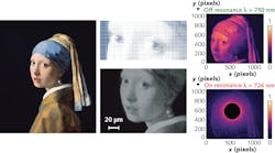
To demonstrate edge detection experimentally on an image, the researchers created a miniature version of the painting Meisje met de parel (by Vermeer) by printing chromium dots onto a transparent substrate. If the image is projected onto the metasurface using off-resonant illumination (750 nm), the original image is clearly recognized. In contrast, if the illumination has the right color (726 nm), the edges are clearly resolved in the transformed image (see figure).
The new optical computing and imaging technique operates at the speed of light and the mathematical operation itself consumes no energy, as it involves only passive optical components. The metasurface can be readily implemented by placing it directly onto a standard CCD or CMOS detector chip, opening new opportunities in hybrid optical and electronic computing that operate at low cost, low power, and small dimensions.
REFERENCE
1. A. Cordaro et al., Nano Lett. (2019); doi.org/10.1021/acs.nanolett.9b02477.

John Wallace | Senior Technical Editor (1998-2022)
John Wallace was with Laser Focus World for nearly 25 years, retiring in late June 2022. He obtained a bachelor's degree in mechanical engineering and physics at Rutgers University and a master's in optical engineering at the University of Rochester. Before becoming an editor, John worked as an engineer at RCA, Exxon, Eastman Kodak, and GCA Corporation.
