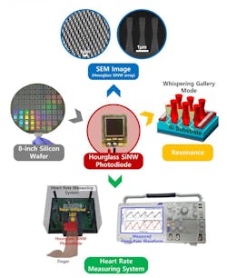
Hourglass nanowire photodiodes extend silicon's near-infrared response
Near-infrared (NIR) light is widely used in optical communications, medical lasers, lidar for self-driving vehicles, and security and surveillance instruments. Many NIR optical systems require photodetectors to capture the signal, but silicon detectors are not effective at wavelengths beyond about 1100 nm. Researchers at Pohang University of Science and Technology (POSTECH) say they have now developed a photodiode with increased absorption of NIR light by using hourglass-shaped nanowires.1 The research team, led by Chang-Ki Baek, developed the shaped silicon nanowires to enhance photoresponse, while still using conventional semiconductor processes for fabrication.
Before their finding, NIR photodiodes made for use beyond 1100 nm were made of chemical materials. These detectors required a separate cooling device to reduce noise, had a high production cost for large-area devices, and were difficult to integrate with electronics. To overcome these difficulties, the team used silicon; the shaped nanowires increase silicon's absorptance of NIR light.
Whispering-gallery resonance occurs in the nanowires; increased absorption occurs as the light passes downward and the hourglass narrows. And because the lower half of the nanowires has a diameter that gradually enlarges downward, the device is more effective at reabsorbing light that was reflected back from the top air/silicon interface. The research team showed that the hourglass-shaped nanowires had 29% higher NIR photoreseponse at a 1000 nm wavelength in comparison to existing silicon photodiodes.
The newly developed photodiode was used in a mobile heart-rate measurement system for demonstration of commercial viability, where the device demonstrated a strong heart-rate signal and less than 1% of the error rate of existing photodiodes.
Source: https://www.eurekalert.org/pub_releases/2019-11/puos-hsn112519.php
REFERENCE:
1. Kihyun Kim et al., Nature Electronics (2019); https://doi.org/10.1038/s41928-019-0317-z.
About the Author
John Wallace
Senior Technical Editor (1998-2022)
John Wallace was with Laser Focus World for nearly 25 years, retiring in late June 2022. He obtained a bachelor's degree in mechanical engineering and physics at Rutgers University and a master's in optical engineering at the University of Rochester. Before becoming an editor, John worked as an engineer at RCA, Exxon, Eastman Kodak, and GCA Corporation.

