Short-wavelength pyrometer improves MOCVD process for microLEDs
MicroLED displays will offer enhanced resolution for mobile devices, television, and augmented/virtual reality (AR/VR) headsets. These emitters are poised to become one of the fastest-growing technologies of the next decade. To capitalize on the microLED opportunity, some LED manufacturers may need to upgrade their existing technology for monitoring temperatures in their metalorganic chemical vapor deposition (MOCVD) reactors. Although the reactors themselves can easily transition from traditional LEDs to microLEDs, the reactors' pyrometers would benefit from being upgraded to enable the precision temperatures necessary for manufacturing microLEDs.
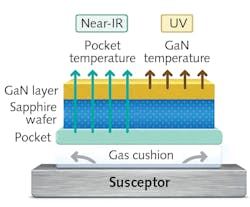
MOCVD reactors have traditionally used optical temperature pyrometers using a measurement wavelength in the near-infrared (near-IR) region, typically around 940 nm, to measure the temperature susceptor that holds the sapphire wafers where the LED quantum wells are being grown. This was state-of-the-art for some time, but in recent years, producers have started to use pyrometers measuring at a shorter wavelength, typically in the range of 400 to 430 nm, for direct measurement of the sapphire wafer itself, because at 940 nm the sapphire wafers are effectively invisible to the pyrometer, so manufacturers can’t precisely measure the wafers’ temperatures during the production process. Instead, the pyrometers measure the carriers’ temperatures and extrapolate from that to estimate the wafers’ temperatures. These estimates continue until the film is deposited on the wafers. This makes the wafers opaque, so the pyrometer now can see them and begin measuring their temperatures directly.
Pyrometers (and associated optics) made by Advanced Energy (Fort Collins, CO) for use at these shorter wavelengths “see” the wafers from the start of production and, says Mark Ritzheimer, the company's senior manager of thermal products, more precisely measure and control the critical early steps of the gallium nitride (GaN)-based deposition process and quantum-well growth. As a result, these pyrometers can provide tighter process control and product uniformity. Contact Ritzheimer at [email protected].

John Wallace | Senior Technical Editor (1998-2022)
John Wallace was with Laser Focus World for nearly 25 years, retiring in late June 2022. He obtained a bachelor's degree in mechanical engineering and physics at Rutgers University and a master's in optical engineering at the University of Rochester. Before becoming an editor, John worked as an engineer at RCA, Exxon, Eastman Kodak, and GCA Corporation.
