Photomultiplier tubes do what other photon counters can’t

Photomultiplier tubes (PMTs) are one of the first devices developed that can detect single photons (Geiger counters can also count individual photons, but only of the gamma-radiation variety). Since the advent of the PMT, many other photon-counting techniques have been invented, including avalanche photodiodes (APDs), single-photon avalanche diode (SPAD) arrays, superconducting nanowire single-photon detectors (SNSPDs), silicon photomultipliers (SiPMs), and microchannel plates (MCPs)—which are actually a compact form of PMT with many parallel channels.
So why is the original, discrete type of PMT still being used? The answer is that it has a combination of qualities that is preferable for numerous applications. This short article provides a bit of background on some commercial examples of PMTs.
Side-on vs. end-on
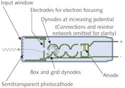
“In a photoemissive detector, light interacts directly with the electrons in the detector material,” explains Ken Corelli, product marketing specialist at Newport (Irvine, CA), an MKS brand. “An absorbed photon frees an electron and the surplus energy gets converted into kinetic energy of an electron (see Fig. 1). Electrons with enough kinetic energy escape from the surface. The electrons emitted in this way produce the cathode photocurrent in PMTs. An applied voltage causes the electrons to flow toward the anode, creating a current that can be proportional to light intensity over six to eight orders of magnitude. The electron multiplier part of a PMT amplifies the photocurrent by secondary emission. This is a low-noise process that produces currents orders of magnitude larger than the initial photocurrent. PMTs are more sensitive than any other detector in the near-UV and visible regions.”
Corelli says that, under the Oriel brand, Newport offers four PMT models which are sourced through a third-party vendor renowned for their detectors. Newport manufactures the PMT power supply, detector housing, and accessories to complete the system for customers.
While Figure 1 shows a schematic of an end-on tube, Oriel’s side-on tubes have similar components arranged in a much-tighter geometry, which makes packaging easier and removes some of the environmental sensitivities of these detectors, notes Corelli. The end-on tubes have larger and more-uniform photosensitive areas; side-on tubes have faster rise times and reach higher responsivities, since most of them use opaque photocathodes, thus avoiding the optical losses associated with the semitransparent photocathodes of the end-on tubes.
“The primary use of our PMTs is in applications where noise-equivalent power (NEP) needs to be as low as possible,” says Corelli. “Examples of these include single-photon microscopy, material characterization, and other single-photon detection experiments.”
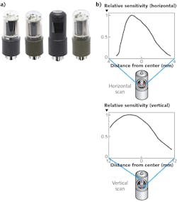
The Oriel 77348 PMT is the most popular device due to its broad spectral range from UV to near-infrared, according to Corelli (see Fig. 2). “The detector also has low NEP with a rated specification 1.2 × 10⁻¹⁶ W Hz-1/2. Another important specification is peak responsivity,” he says. “This results in a larger amplified signal per incident photon, making this PMT ideal for very low-light conditions. A popular application for this PMT is single-photon microscopy, because it requires extremely low noise and light signals while delivering significant current amplification. The optional PMT housing ensures a secure fit with Oriel monochromators, eliminating undesired stray light.”Keeping with the single-photon microscopy application, Corelli notes that Oriel’s PMTs are able to detect single photons, whereas other technologies such as SiPMs, APDs, SPADs, and so on cannot due to excess noise factors inherent in their designs.
The stability of the electron-multiplying process in a PMT depends on the electrons following precise trajectories. Magnetic fields can affect the directions of such electron flow in a significant manner, since the tubes are physically large. This is particularly noticeable for end-on PMTs, says Corelli. “To greatly improve measurement reproducibility in single-photon microscopy, both of our PMT housings have significant magnetic shielding built-in by design,” he adds. “They can either be rod-mounted on an optical table for free-space measurements, or secured by the built-in mounting flange to other Oriel branded products.”
Huge variety of PMTs
Photomultiplier tubes have many advantages such as high-speed response, a large effective area, and ultrahigh sensitivity for weak light detection, notes Jake Li, business development manager at Hamamatsu (Hamamatsu City, Japan), a company especially well known for its long history producing PMTs in large OEM quantities and in small custom batches.
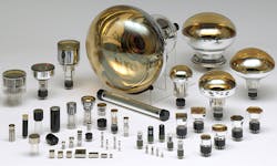
One example of the latter is the extremely large type of PMT produced by Hamamatsu for (indirect) neutrino detection (see Fig. 3), in which large 3D arrays of these PMTs are placed in water or ice detect the presence and direction of neutrinos via the Cherenkov light they emit as they interact with matter. The 20 in. PMTs are used in the Kamiokande and SuperKamiokande neutrino observatories in Japan (placed in water), as well as the IceCube neutrino observatory at the South Pole (embedded in a 1 km3 cube of ice). Hamamatsu is continually improving the collection efficiency of these PMTs—from an efficiency of 40% to 50% for the Kamiokande observatory, to 70% for SuperKamiokande, to 90% planned for a future HyperKamiokande observatory.Ruggedized high-temperature PMT. These PMTs employ a high-temperature bialkali photocathode and feature stable operation and long life at temperatures up to 200°C. Their electrodes’ supporting structures are especially designed so that these PMTs can withstand severe environmental conditions such as those found in oil-well logging, geological exploration, and aerospace applications.
GaAsP/GaAs/InGaAs PMT. Hamamatsu has developed III-V semiconductor photocathodes such as GaAsP, GaAs, and InGaAs to achieve higher sensitivity. PMTs with these photocathodes are receiving a great deal of attention in life science fields such as laser scanning microscopy and flow cytometry (FCM), where it is necessary to detect ultraweak light.
HPD. The hybrid photodetector (HPD) is a PMT with a semiconductor element built into the electron tube. Features offered by HPDs include extremely small fluctuations during the signal multiplication, single photoelectron resolution, and excellent time characteristics. These features make the HPD useful for a wide range of applications including laser scanning microscopy, fluorescence lifetime imaging microscopy (FLIM), fluorescence correlation spectroscopy (FCS), and light detection and ranging (lidar).
Micro PMT. The micro PMT is the world’s smallest and lightest photomultiplier tube, says Li, and it can be mass-produced using semiconductor manufacturing technology. Due to its smaller size and its performance comparable to conventional PMTs, it can help reduce the size of instruments without compromising their performance.
A typical conventional PMT is a small tube with a diameter of 1.5 cm and a length of about 5 cm, and its components—the photocathode, dynodes, and anode—are housed in a vacuum glass tube. Due to the large number of parts and a manufacturing process that requires the work of highly skilled technicians, there was a limit to miniaturization and mass production. “As a solution, we introduced the micro-PMT, which can be mass-produced more easily than conventional PMTs,” notes Li.
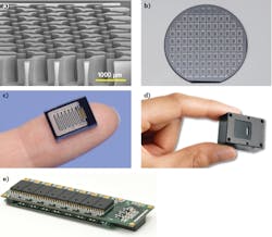
The micro-PMT has a three-layer structure in which a silicon substrate is sandwiched between two glass substrates. Dynodes are produced by deep etching (900 µm) on a silicon substrate using technology developed for MEMS device production (see Fig. 5a). Vacuum airtightness is achieved by firmly bonding a silicon substrate and a glass substrate using anode bonding, also a MEMS technology. Through this process, a wafer-shaped product (see Fig. 5b) containing about 100 micro-PMTs is completed. Finally, the wafer is separated into chips through a dicing process; each chip measures about 10 mm (W) × 13 mm (H) × 2 mm (D), which is small enough to fit on a fingertip (see Fig. 5c), and weighs about 0.5 g.The characteristics of micro-PMTs are similar to those of conventional PMTs; at an applied voltage of 900 V, a micro-PMT’s gain is about 2 million, and its anode output pulse has a 1.2 ns rise time and 1.7 ns fall time. In addition, micro-PMTs have the advantage of having a lower dark current than conventional PMTs due to their small photocathode area.
Hamamatsu has also developed the technology to miniaturize modules, and recently commercialized an ultracompact micro-PMT module that includes a high-voltage power supply and a voltage divider circuit (see Fig. 5d). Due to the module’s small size, Hamamatsu can also create arrays by lining up several modules like solid-state detectors (see Fig. 5e).
Micro-PMTs in point-of-care testing
As an example of how micro-PMT technology can be applied, Li points to the healthcare industry. Using small analyzers or rapid diagnostic kits, point-of-care testing (POCT) brings medical tests to a patient’s location and obtains the same results as a test performed in a hospital laboratory. There are tests performed at a patient’s bedside in hospitals and wards, as well as patient monitors in hospital emergency centers and operating rooms. POCT is attracting attention as a possible feature incorporated into doctors’ examination rooms in the future. At present, PMTs are used in large blood test analyzers, but by using micro-PMTs, point-of-care devices with the same performance as their larger counterparts can be developed. Additionally, introducing PMTs’ advantages into POCT analyzers can boost performance.
About the Author
John Wallace
Senior Technical Editor (1998-2022)
John Wallace was with Laser Focus World for nearly 25 years, retiring in late June 2022. He obtained a bachelor's degree in mechanical engineering and physics at Rutgers University and a master's in optical engineering at the University of Rochester. Before becoming an editor, John worked as an engineer at RCA, Exxon, Eastman Kodak, and GCA Corporation.


