The semiconductor industry has grown to become one of the largest and most important industries in the world. Silicon is the building block of memory chips, computer processors, transistors, and virtually all other electronics that impact us all on a daily basis. It is an element with very special properties: the most notable is that it is a semiconductor, conducting electricity under some conditions and acting as an insulator under others. Silicon’s electrical properties can be modified through a process called doping, making it an ideal material for making transistors.
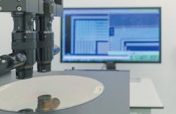
The entire silicon manufacturing process takes six to eight weeks and is performed in highly specialized semiconductor foundries, or fabs. Silicon inspection (see Fig. 1) can be a challenging problem for silicon and semiconductor manufacturers in terms of pattern alignment, pattern defect inspection, and edge-position bonding inspection. During the manufacturing process, foreign particles and defects may appear on the top, bottom, inside, or in between the wafers. And, as the thickness of wafers gets smaller, backside defects are becoming more important to detect. These include air pockets, microcracks, and other fine features caused by photonic emissions. Defects do not initially affect the chips’ functionality, but they do end up affecting the chips’ reliability—important in critical devices. Quality control is of paramount importance to silicon manufacturers.
Camera-based inspection
CCD and CMOS cameras have traditionally been used for silicon surface inspection. The silicon sensors in these cameras have a wavelength response from 350 to 1000 nm. Deep-depleted devices have just about high-enough quantum efficiency (QE) to see the shortest wavelengths emitted by silicon electro- or photoluminescence, observing photon emissions with energy transitions above the silicon bandgap. However, such devices need long integration times and do not allow the observation of intraband emissions above 1100 nm, where this emission is most intense, so they can only be used for offline front-side inspection.
Moving into shortwave-infrared (SWIR)
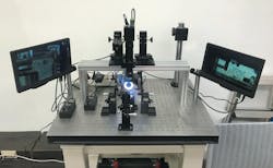
Silicon has an interesting property in which it becomes translucent at wavelengths >1150 nm. This makes indium gallium arsenide (InGaAs)-based cameras extremely interesting for the monitoring of wafer-bonding processes because, seen in SWIR, pure silicon is transparent at room temperature, while heavily doped silicon becomes more and more opaque as the temperature increases (>200°C). Because of this property, two-dimensional focal-plane array (FPA) InGaAs cameras are ideal for detecting wafer defects, particles, voids, or other imperfections between two bonded wafers (see Fig. 2).InGaAs-based cameras are capable of detecting light between 900 and 1700 nm. Subbandgap emissions involving chemical impurities, physical defects, and deep traps and other recombination centers are also not observable; backside analysis (necessary with the use of multilevel metals preventing photon emission from the front side of the wafer) requires transmission of the emission through the silicon substrate.
With the use of filters, InGaAs cameras can limit the wavelength range they detect to only those for which the wafers are translucent, making these cameras ideal to use for wafer inspection, edge-position bonding, and imaging of wafer alignment marks, microcracks, edge crack inspection, photon emission, and other fine features.
SWIR cameras can be used to inspect the quality of pure semiconductor material (usually silicon) after ingot growth. Furthermore, ingots that are subsequently sliced into wafers can in a similar way be inspected for defects or cracks. The impurities inside the brick or ingot can cause damage to the production equipment when the ingots are further processed into wafers. Wafers are then processed into optoelectronic and electronic components. For semiconductor devices, the final processing step is dicing of the wafer into single chips, and here a SWIR camera is used for alignment of the saw blade or laser. They can also be used to improve yield in MEMS manufacturing by performing sealing inspection, detection of bubbles or breaches, device defect inspection, and critical-dimension and overlay measurements. For wafer-level packaging (WLP), which is a technique that combines wafer manufacturing and device encapsulation technologies, SWIR cameras can be used for multiple quality assessment tasks.
SWIR photon-emission microscopy (PEM) is an established, passive fault-localization technique for microelectronic failure analysis. Photon emission occurs when an electron makes a transition from a higher energy state to a lower energy state. All or part of the energy difference is emitted as electromagnetic radiation. Photon emission from defects is generally associated with forward and reverse biased p-n junctions, transistors in saturation, or dielectric breakdown.
Not all InGaAs cameras are equal
SWIR cameras have been around for more than 30 years. Over this period, the quality and sensitivity of sensors has substantially improved, resolution has increased, pixel pitch has gotten smaller, and cooling has been introduced to enable longer exposure times. Cameras have become more compact and can run faster. The ones that are of most interest to the silicon inspection industry are the ones that image the smallest defects, run at the fastest frame rates, and image the widest field of view.
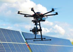
Operating on a 24/7 production line, these cameras also need to be very reliable, rugged, and compact. Embedded in instruments, the cameras heat up, so stabilized cooling is required for consistent results. Other important considerations include resolution and pixel size; a wider field of view to enable higher volumes of silicon to be inspected; and faster frames rates to enable higher throughput. An InGaAs camera such as Raptor Photonics’ Owl 1280 provides all these features; an added bonus is that it also offers a visible extension, offering 600–1700 nm imaging and essentially replacing the need for two camera systems. This camera has already been integrated by a number of OEMs into their silicon inspection systems.Silicon inspection has become an integral process in the semiconductor industry. Whether detecting cracks and defects on silicon wafers or solar-cell panels (see Fig. 3), or for achieving a failure analysis of integrated circuits, detecting defects helps to improve yields and overall productivity. InGaAs cameras are becoming an increasingly important enabling tool.
Mark Donaghy | VP of Sales and Marketing, Raptor Photonics
Mark Donaghy is VP of Sales and Marketing at Raptor Photonics (Larne, Northern Ireland).


