Large-area CMOS imaging technology delivers quantum efficiency over 90%

Feb. 22, 2021
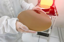
LACera CMOS imaging technology has uses in applications such as next-generation genomics, astronomical photometry, and ultra-high-resolution x-ray and electron imaging.

LACera CMOS imaging technology has uses in applications such as next-generation genomics, astronomical photometry, and ultra-high-resolution x-ray and electron imaging, all of which require CMOS sensors and cameras with low light sensitivity and speed. LACera delivers >90% quantum efficiency and the company’s low-noise architecture with up to 18-bit readout, and will be featured in the company’s next-generation CMOS cameras to be announced later in 2021. X-ray, extreme ultraviolet (EUV), and visible-near-infrared (VIS-NIR) versions will be available. 

Teledyne Imaging

Waterloo, ON, Canada
largeareacmos.com

GET PRICING

Sponsored Recommendations

Brain Computer Interface (BCI) electrode manufacturing

Jan. 31, 2025
Learn how an industry-leading Brain Computer Interface Electrode (BCI) manufacturer used precision laser micromachining to produce high-density neural microelectrode arrays.

Electro-Optic Sensor and System Performance Verification with Motion Systems

Jan. 31, 2025
To learn how to use motion control equipment for electro-optic sensor testing, click here to read our whitepaper!

How nanopositioning helped achieve fusion ignition

Jan. 31, 2025
In December 2022, the Lawrence Livermore National Laboratory's National Ignition Facility (NIF) achieved fusion ignition. Learn how Aerotech nanopositioning contributed to this...

Nanometer Scale Industrial Automation for Optical Device Manufacturing

Jan. 31, 2025
In optical device manufacturing, choosing automation technologies at the R&D level that are also suitable for production environments is critical to bringing new devices to market...

Voice your opinion!

To join the conversation, and become an exclusive member of Laser Focus World, create an account today!