IR DETECTORS: Semiconductor processing technology improves resolution of infrared arrays
ALAN HOFFMAN
Infrared systems are requiring higher resolution than ever before, and many applications, such as wide-area surveillance and astronomy, are demanding more pixels on their IR focal planes to capture more information. Fortunately, detector manufacturers have been able to keep up by making larger and denser infrared arrays. Array size has been increasing at an exponential rate, following a Moore’s Law grow path for the last 25 years, with the number of pixels doubling every 19 months (see Fig. 1). Arrays are expected to exceed 4K × 4K format-16 million pixels-this year, about a year later than the Moore’s Law prediction.
A primary enabling technology for this spectacular growth also enables the ever-increasing power of computers: semiconductor processing. The initial observation by Intel (Santa Clara, CA) founder Gordon Moore that became Moore’s Law was based on the rapid improvements in silicon foundry operations. The availability of larger wafers of single-crystal silicon, smaller feature sizes, and larger die size all contributed to the exponential growth. The larger die sizes became possible as wafer fabrication facilities reduced particle contamination and other sources of defects and yields increased. These same factors have contributed to the growth of IR arrays.
Device construction
Most modern IR devices are fabricated from two pieces of material-a detector array made from compound semiconductor materials such as indium antimonide (InSb) or mercury cadmium telluride (HgCdTe); and a silicon signal-processing chip called a readout integrated circuit (ROIC). The ROIC amplifies the signal from each detector element, performs processing functions such as integrating the signal over a period of time, and then reads out the signal by multiplexing the signals of thousands of pixels onto a few output lines. Although ROICs are considered “mixed mode” devices-that is, they have analog and digital components-they are fabricated using virtually the same transistor process as computer chips.
The Moore’s Law improvement in the size and processing power of readout chips is a direct result of improvements in digital computers. The increase in size of the detector arrays is a collateral effect of understanding better crystal growth techniques, better photolithography, and cleaner processing environments, all transferred from silicon foundries to the “exotic” semiconductors used for IR detectors.
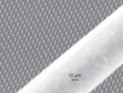
The two elements of the IR sensor form a stacked structure, called a sensor chip assembly (SCA), which connects the IR detector array to the ROIC using a hybridization process. Although similar to the flip-chip technology used by the computer industry, IR hybridization requires millions of indium “bumps” to be connected on each die, one bump for each pixel fabricated on an 8-µm center, with center-to-center spacing on the order of 10 to 20 µm (see Fig. 2).During hybridization, the detector and ROIC die are positioned parallel to one another and then pressed together with a force that can exceed 200 lb. Alignment and parallelism accuracies must be better than 1 µm for all the indium bumps to make reliable electrical and physical connections. Remarkably, experienced IR-detector manufacturers typically connect 99.99% of the indium bumps even on megapixel arrays.
Cooling stresses
The final hurdle that IR-detector manufacturers must overcome in making large arrays is the physical contraction that occurs when detectors are cooled to reduce thermally generated noise. Because detector materials such as InSb and HgCdTe have coefficients of thermal expansion different from those of silicon ROICs, mechanical stress can build up in the SCA during cooling, ripping apart indium bump contacts or even shattering the detector and ROIC die. Manufacturers have come up with a variety of techniques to prevent this.
Some detector materials such as InSb must be thinned to approximately 10 µm to efficiently detect IR light. The thinned crystal becomes elastic, enabling expansion and contraction with the silicon ROIC without damage to the detector or the indium bumps. This makes InSb arrays naturally scalable to large formats without extra processing.
Other detector crystals, most notably HgCdTe, are too brittle to withstand such stretching, even when thin. The usual strategy in this case is to force the ROIC to contract in compliance with the detector. The ROIC-sometimes thinned to make it more compliant-is bonded to a stiff material that has a coefficient of thermal expansion similar to that of the detector.
Yet another strategy is to manufacture the detectors on a silicon substrate so the substrates of the detector and ROIC are thermally matched. This has been successfully accomplished with HgCdTe detectors, with the added bonus that wafers of silicon can be made larger and cheaper than wafers of cadmium zinc telluride (CdZnTe), the standard substrates for these detectors.
Astronomical proportions
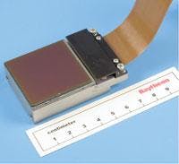
As recently as five years ago it was widely believed that either the hybridization process or the thermal-contraction mismatch would limit the size of IR arrays to no more than one megapixel. However, IR arrays as large as 2K × 2K pixels with 99.99% good indium bump interconnects are now commercially available (see Fig. 3). Raytheon incorporates a unique “GREATOP” structure to constrain ROIC thermal expansion and has not observed any degradation from cooling the SCAs despite thermal cycling more than 500 times to 80 K (-193°C).Even the 4 million pixels of a 2K × 2K SCA are not enough for some applications, however. Astronomers in particular desire more pixels so they can view a wider area of the sky with better resolution. Because telescope observation time is precious and new telescopes are expensive, the obvious strategy is to pack more pixels onto the focal plane. A good example of this is the VISTA (Visible and Infrared Telescope for Astronomy) 4-m telescope being constructed in Chile by astronomers from the United Kingdom.
The mission is to survey the entire sky in the Southern Hemisphere at four IR wavelengths. Quick calculations indicate a need for more than 60 million IR pixels to complete the initial survey in six years.1 In addition, because the VISTA telescope is a relatively fast f/3 optical system, every detector element must be within 12 µm of the focal point,
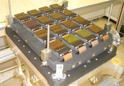
To create a focal plane with the required accuracy and magnitude, Raytheon manufactured a 4 × 4 mosaic of 2K × 2K HgCdTe SCAs and assisted in assembling into the final focal-plane configuration (see Fig. 4). With 67 million pixels, this is currently the world’s largest IR focal plane.Looking ahead
What is the future of IR arrays? Sensor chip assemblies will certainly be available with more features, such as automatic gain control and signal-processing functions, including noise filtering. Features that simplify IR focal-plane input/output, such as generation and regulation of DC voltages; generation of complex timing signals; and analog-to-digital conversion of the output signal, are already being incorporated into the most advanced ROICs. A feature-rich infrared SCA follows the trend toward more-complex but more-user-friendly computer chips.
Array sizes will continue to increase but perhaps at a rate that falls below the Moore’s Law curve. An increase in array size is already technically feasible: crystal growers are growing ever-larger wafers of IR-sensitive materials; silicon foundries used for ROICs continue to improve yields; mechanical engineers have designed hybridization equipment capable of greater force and accuracy. However, the market forces that have demanded larger arrays are not as strong now that the megapixel barrier has been broken.
For many systems, such as night-vision goggles, the IR image is viewed by the human eye, which can discern resolution improvements only up to about one megapixel, roughly the same resolution as high-definition television. Most high-volume applications can be completely satisfied with a format of 1280 × 1024 or less. Although wide-area surveillance and astronomy applications could make use of larger formats, funding limits may prevent the exponential growth that was seen in past decades.
Perhaps most important to users and instrument builders is that IR detectors will continue to come down in cost. Currently large commercial, high-performance SCAs cost about 10 cents per pixel. Off-the-shelf IR arrays of more modest sizes (less than 1 megapixel) are already only a few cents per pixel. Future cost improvements will drive exponential growth in IR applications, which we will undoubtedly see over the next decade.
REFERENCES
1. www.vista.ac.uk.
ADDITIONAL INFORMATION
“Modern Infrared Detectors and System Applications” is a five-day short course at the University of California, Santa Barbara, that includes hands-on laboratories and IR-camera demonstrations in addition to classroom instruction. The next class is June 19-23. Contact: www.extension.ucsb.edu.
Georgia Tech offers several infrared courses throughout the year among its “Defense Technology” short courses. Contact: www.pe.gatech.edu.
“Infrared Imaging Systems and Applications” is a three-day short course at the University of California, Los Angeles. The next class is March 13-15. Contact: www.uclaextension.edu.
The University of Michigan generally offers two infrared courses each summer although at press time no dates had been announced for 2006. Contact: bulletin.engin.umich.edu.
Alan Hoffman coordinates a short course on infrared technology at the University of California, Santa Barbara and is a Fellow at Raytheon Vision Systems, 75 Coromar Dr., Goleta, California 93117; e-mail: [email protected]; www.raytheon.com.


